
2 layers48.2 × 20.3 mm

 ciniml/fpga_samples31
FPGA samples
DE0Header PmodAdapter is an open-source printed circuit board by ciniml, from the ciniml/fpga_samples repository on GitHub, published under the BSL-1.0 licence. It is a 2-layer board of 91.4 × 45 mm with 17 parts on 41 nets, routed with 295 tracks and 86 vias.
It is built around the AMS1117-3.3. Its parts include 7 connectors, 6 capacitors and 1 IC. It belongs with the fPGA and programmable logic boards of this library.
Raspberry Pi カメラ (15 ピン 1.0 mm FFC, 2 レーン MIPI CSI-2) を Pmod 1 個につなぐ変換基板。
FPGA 側はソフト D-PHY (eda/csi_capture, rtl/csi2)。KiCad 10。
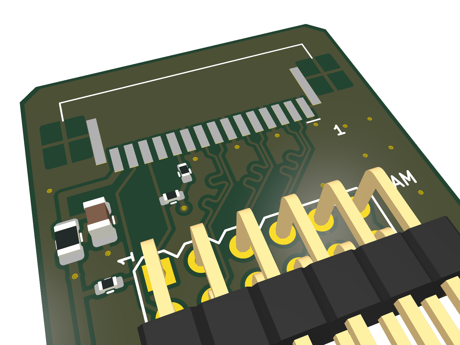
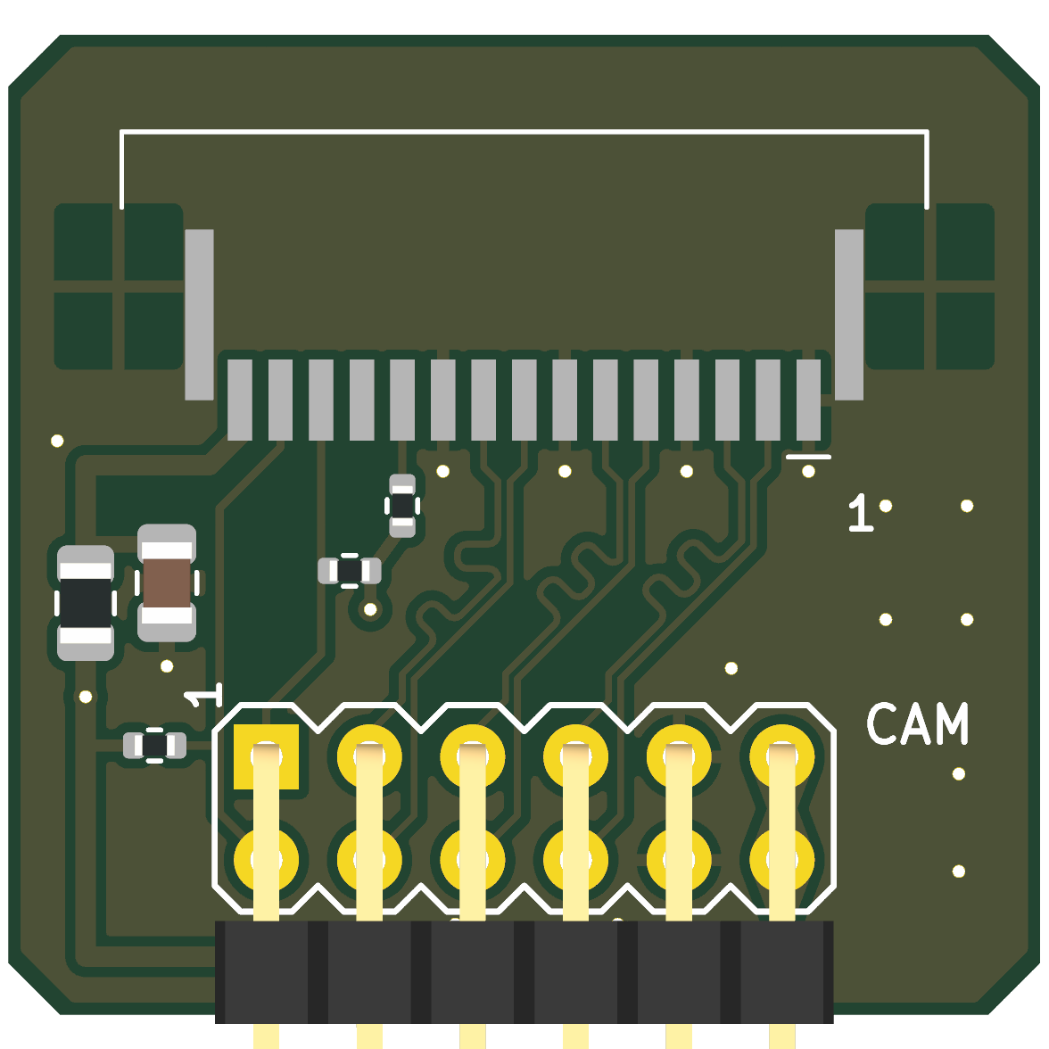
状態: 設計のみ (未発注・実機未確認)。ERC / DRC (回路図との一致を含む) はエラー 0。
Conn_Pmod_Spec_B_Thin)、基板下端Local/local.pretty)。基板上端寄り、ケーブルは上から挿す (ハウジング前端は基板端から 2.5 mm 内側)。
rev A の当初は TE 1-84952-5 だったが JLC 在庫が 1 個のため変更 (接点列の位置は同じ = 配線は無変更)| Pmod | 信号 | FFC | Tang Primer 25K (pmod0) |
|---|---|---|---|
| 1 / 7 | SCL / SDA | 13 / 14 | F5 / G5 |
| 2 / 8 | CLK P / N | 9 / 8 | G7 / G8 |
| 3 / 9 | D1 P / N | 6 / 5 | H8 / H7 |
| 4 / 10 | D0 P / N | 3 / 2 | H5 / J5 |
| 5, 11 | GND | 1, 4, 7, 10, MP | |
| 6, 12 | 3.3 V | 15 (F1 経由) | |
| — | CAM_GPIO | 11 | R3 で 3.3 V へ (カメラは Pmod 給電で即起動) |
| — | CAM_CLK | 12 | 未接続 |
FFC のピン配置は Raspberry Pi 4 公式回路図 (J3 CAMERA) で確認。Pmod 上の並び (CLK, D1, D0) は
FFC 上の並びと同じ順にして、差動対が交差しないようにしてある (FPGA の pins.cst も同じ割り当て)。
FPGA 側の定義は mod/pmod_rpi_camera/pmod_pins.csv。
公式資料から確認済み:
同じコネクタ同士を両端逆面のケーブルでつなぐと、基板の向きによらず ピン n ↔ ピン n になる (3.3V は 15 番どうし、GND は 1 番どうし)。カメラに付属の標準ケーブルを使うこと。 両端が同じ面の社外ケーブルでは逆転し、本基板の 3.3V (15 番) がカメラの GND に当たる (F1 が制限する)。
念のための確認 (カメラをつながずに): ケーブルを J2 に挿し、ケーブル反対端の導体 1 番と Pmod の GND (5/11 番) の 導通をテスタで見る。導通すれば正しい。
tools/build.sh が ERC / DRC (回路図との一致、ベタ再充填込み) を通してから fab/ を作る:
| ファイル | 内容 |
|---|---|
fab/Pmod_RPiCamera_gerber.zip | ガーバー (F/B Cu, Mask, Silk, F.Paste, Edge) + ドリル (PTH/NPTH 別) |
fab/Pmod_RPiCamera_bom.csv | 部品表 (LCSC 番号、MPN 付き) |
fab/Pmod_RPiCamera_pos.csv | 実装位置 (表面のみ、原点は基板左下) |
fab/jlc/Pmod_RPiCamera_jlc_bom.csv, ..._jlc_cpl.csv | JLCPCB 実装用 BOM / CPL (LCSC 番号のある部品のみ。J1 は手はんだ想定で除外) |
fab/lcsc/Pmod_RPiCamera_lcsc_5pcs.csv | LCSC 部品購入用 (5 枚分、J1 含む)。tools/lcsc_order.py N で N 枚分を作り直す (LCSC に問い合わせて最小発注数・単価・在庫を反映、要ネットワーク) |
fab/Pmod_RPiCamera_schematic.pdf | 回路図 |
fab/*.png | 3D レンダリング |
fab/erc.rpt, fab/drc.rpt | 検査結果 (ライブラリ表の警告はヘッドレス環境由来) |
回路図・基板の初版は tools/gen_sch.py / tools/gen_pcb.py で生成し、その後 KiCad で手を入れている
(rev A: P 側の等長化ミアンダ、ティアドロップ、ロゴ、J2 を SFW15R-1STE1LF に変更、LCSC 番号)。KiCad のファイルが正
(スクリプトは初版の TE コネクタのまま)。tools/build.sh は既定で
現状のファイルを検査して出力するだけ。--regen を付けるとスクリプトから作り直し、KiCad での修正は消える。
| Ref | 部品 | LCSC | 備考 |
|---|---|---|---|
| J1 | 2x6 2.54 mm 直角ピンヘッダ | — | 手はんだ想定。JLC で載せるならピン長・本体寸法をフットプリントと照合 (候補 C41417354) |
| J2 | Amphenol SFW15R-1STE1LF | C3168538 | 在庫 9,155、Extended |
| F1 | RUILON SMD0805P050TF (I_hold 0.5 A, 6 V) | C20978 | 代替 Littelfuse 0805L050WR (C207022) |
| C1 | Samsung CL21A106KAYNNNE (10 µF 25 V X5R 0805) | C15850 | Basic |
| R1, R2 | UNI-ROYAL 0402WGF2201TCE (2.2 kΩ) | C25879 | Basic |
| R3 | UNI-ROYAL 0402WGF1002TCE (10 kΩ) | C25744 | Basic |
JLC の配置プレビューで J2 の回転・原点を確認すること (KiCad のフットプリント原点は接点列の中心。 JLC 側のモデル原点と違う場合はオフセットが出る)。J2 の 3D モデルは無い (3D 画像に J2 は写らない)。
../../README.md)| Qty | Value | Footprint | References |
|---|---|---|---|
| 4 | 100n | Capacitor_SMD:C_0402_1005Metric | C3, C4, C5, C6 |
| 2 | MountingHole_2.7mm_M2.5_ISO7380 | MountingHole:MountingHole_2.7mm_M2.5_ISO7380 | H1, H2 |
| 1 | 10u | Capacitor_SMD:C_0805_2012Metric | C1 |
| 1 | 22u | Capacitor_SMD:C_0805_2012Metric | C2 |
| 1 | 2x20 female 2.54 (to Dock J3) | Connector_PinSocket_2.54mm:PinSocket_2x20_P2.54mm_Vertical | J1 |
| 1 | AMS1117-3.3 | Package_TO_SOT_SMD:SOT-223-3_TabPin2 | U1 |
| 1 | EXT1 2x2 | Connector_PinHeader_2.54mm:PinHeader_2x02_P2.54mm_Vertical | J6 |
| 1 | EXT2 2x3 | Connector_PinHeader_2.54mm:PinHeader_2x03_P2.54mm_Vertical | J7 |
| 1 | PMOD A (pmod3) | Connector_PinSocket_2.54mm:PinSocket_2x06_P2.54mm_Horizontal | J2 |
| 1 | PMOD B (pmod4) | Connector_PinSocket_2.54mm:PinSocket_2x06_P2.54mm_Horizontal | J3 |
| 1 | PMOD C (pmod5) | Connector_PinSocket_2.54mm:PinSocket_2x06_P2.54mm_Horizontal | J4 |
| 1 | PMOD D (pmod6) | Connector_PinSocket_2.54mm:PinSocket_2x06_P2.54mm_Horizontal | J5 |
| 1 | logo | local:logo | LOGO1 |


pascallanger/DIY-Multiprotocol-TX-Module
Multiprotocol TX Module (or MULTI-Module) is a 2.4GHz transmitter module which controls many different receivers and models.

fossasia/pslab-hardware
PSLab Hardware Design and Schematics https://pslab.io


MaltWhiskey/Mega-Cube
16x16x16 PL9823 Cube with Teensy 4.0 and FlexIO driver


shamansystems/Cheap-FOCer-2
Low-Cost Motor Controller based on the VESC 6
It measures 91.4 × 45 mm and has 2 copper layers, 1.6 mm thick.
17 parts, built around the AMS1117-3.3. The full list of its parts is on this page, with links to each part's symbol and footprint where PCBKit's library has them.
From the ciniml/fpga_samples repository on GitHub, at the commit this page was made from: the board is eda/targets/tangprimer25k/hw/DE0Header_PmodAdapter/DE0Header_PmodAdapter.kicad_pcb and its schematic eda/csi_capture/hw/Pmod_RPiCamera/Pmod_RPiCamera.kicad_sch. PCBKit opens the board in the browser, with nothing to install.
Its repository publishes it under the BSL-1.0 licence: you may reuse it on that licence's terms (keep the author's notice, and for a copyleft licence share your changes alike).