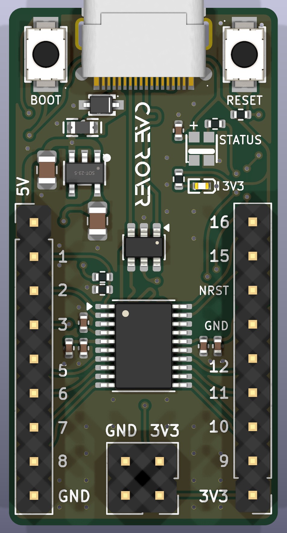
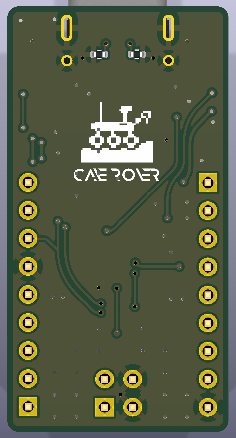
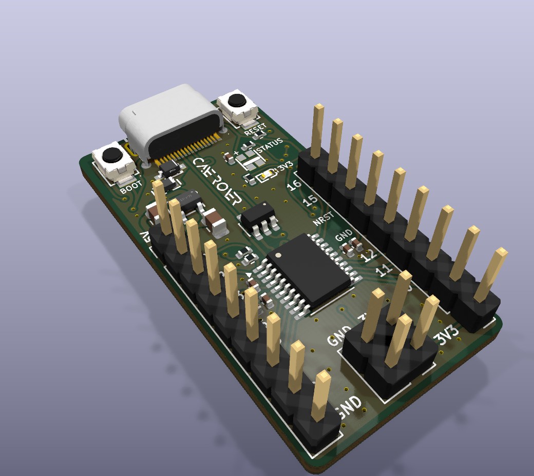
Arm tiny pcb is an open-source printed circuit board by Chicken-Fried, from the Chicken-Fried/STM32-NanoCortex repository on GitHub, published under the CERN-OHL-S-2.0 licence. It is a 2-layer board of 20 × 38.5 mm with 29 parts on 32 nets, routed with 783 tracks and 73 vias.
It is built around the STM32F042F6P6, USBLC6-2SC6 and SKRKAEE020, with the 16-213/BHC-AN1P2/3T, GT-USB-7025 and JK-SMD0603-050-6 among its other parts. Its parts include 8 capacitors, 7 resistors, 3 diodes, 3 connectors and 2 ICs. It belongs with the microcontroller boards boards and the STM32 boards of this library.
A practical, standalone 32-bit development board (20 mm × 38.5 mm), inspired by the minimalist philosophy and straightforward nature of the Arduino ATtiny, but optimized for comfortable benchtop development (devboard). Powered by the STM32F042 (ARM Cortex-M0) with native crystal-less USB-C, a TVS-protected USB input and a ceramic-only 3.3 V power stage.
🌟 Why This Project?
This board was born at the intersection of academic learning, curiosity, and maker passion:
Bridging Theory and Practice: Taking electronic engineering coursework (schematic design, component selection, signal integrity, PCB layout) and applying it to a tangible, physical board.
Stepping into 32-bit Microcontrollers: Moving beyond traditional 8-bit platforms (AVR, ATtiny) into the modern ARM Cortex ecosystem.
Fun & Hobby: A passion-driven learning playground to experiment with USB stacks, low-power modes, and embedded programming.
Giving Back to Open Source: Providing a clean, accessible, and minimal reference design for students, hobbyists, and makers.
Real-World Project Stepping Stone: Serving as the core validation platform for three concrete engineering builds: a dedicated drone telemetry/control subsystem, an audio synthesizer with active analog op-amp (AOP) filtering, and a digitally controlled $\ge$ 40W USB-PD / Buck converter power stage.
🔌 Crystal-less USB-C: Employs the internal 48 MHz oscillator (HSI48) paired with Clock Recovery System (CRS) synchronized directly to USB frames—zero external crystal required.
🚀 Zero-Programmer Flashing (Native DFU): Factory ROM USB bootloader built-in. Hold the BOOT button, plug in the USB-C cable, and flash directly with STM32CubeProgrammer or dfu-util—no ST-Link or external programmer strictly required!
📐 Compact Devboard Layout (20 mm × 38.5 mm): Slim form factor with two 9-pin I/O headers on the long sides, and the BOOT / RESET buttons on each side of the USB-C connector.
🛡️ Enhanced USB Protection:SD05-01FTG TVS diode on VBUS, USBLC6-2SC6 on the data lines and a 500 mA resettable polyfuse.
⚡ Stable 3.3 V:ME6211C33M5G-N low-dropout, low-quiescent-current LDO, stable with small ceramic capacitors (no more tantalum).
💡 Two Indicator LEDs: a red 3V3 power LED and an addressable WS2812B-2020-V6 RGB STATUS LED driven from PA0 (native 3.3 V operation with dedicated 100 nF decoupling capacitor C8).
🎛️ Dual Tactile Buttons: On-board RESET and BOOT tactile switches for instant programming mode entry.
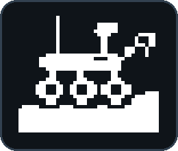
🛰️ CaveRover Branding: Features the official 8-bit pixel art CaveRover rover silkscreen emblem and futuristic Anurati typographic markings directly on the PCB.
🛠️ Open-Source & DIY Ready: Standard 2-layer PCB design rules for affordable fabrication and assembly (e.g. JLCPCB).
📋 Specifications
Parameter
Specification
Microcontroller
STM32F042F6P6 (TSSOP-20)
Core Architecture
ARM 32-bit Cortex-M0 @ up to 48 MHz
Flash / SRAM
32 KB Flash / 6 KB SRAM
Operating Voltage
3.3 V logic (Dual power rails exposed: 5 V via USB-C + 3.3 V regulated)
⚠️ Important Note on PB8 / BOOT0 (GPIO1): Pin 1 of the TSSOP-20 package is shared between BOOT0 and PB8. It is pulled down to GND via $R_7$ (10 kΩ) for normal Flash execution. Any external circuitry attached to GPIO1 that pulls this pin HIGH at reset will force the microcontroller into native USB DFU bootloader mode.
💡 Internal Signals & ADC Allocation:
PA0 is dedicated internally to the WS2812B-2020-V6 RGB status LED via $R_6$ (330 Ω). Consequently, analog channel ADC_IN0 is reserved for on-board LED operation. 7 external ADC channels remain freely available on the headers (PA1 to PA7).
NRST is wired to the tactile RESET button with a 100 nF debounce capacitor and routed to J2 pin 7 for full debugger control.
🔌 Serial Communication (USART1 vs USART2):
For user serial communication (e.g. drone CRSF/SBUS telemetry, debug console, GPS), use USART2 (PA2/PA3) on header J1.
On the STM32F042 TSSOP-20 package, USART1 (PA9/PA10) shares physical pins 17 & 18 with native USB Full-Speed (PA11/PA12, USB_DM/USB_DP). When USB is active, USART1 cannot be used simultaneously.
🛠️ Hardware Overview
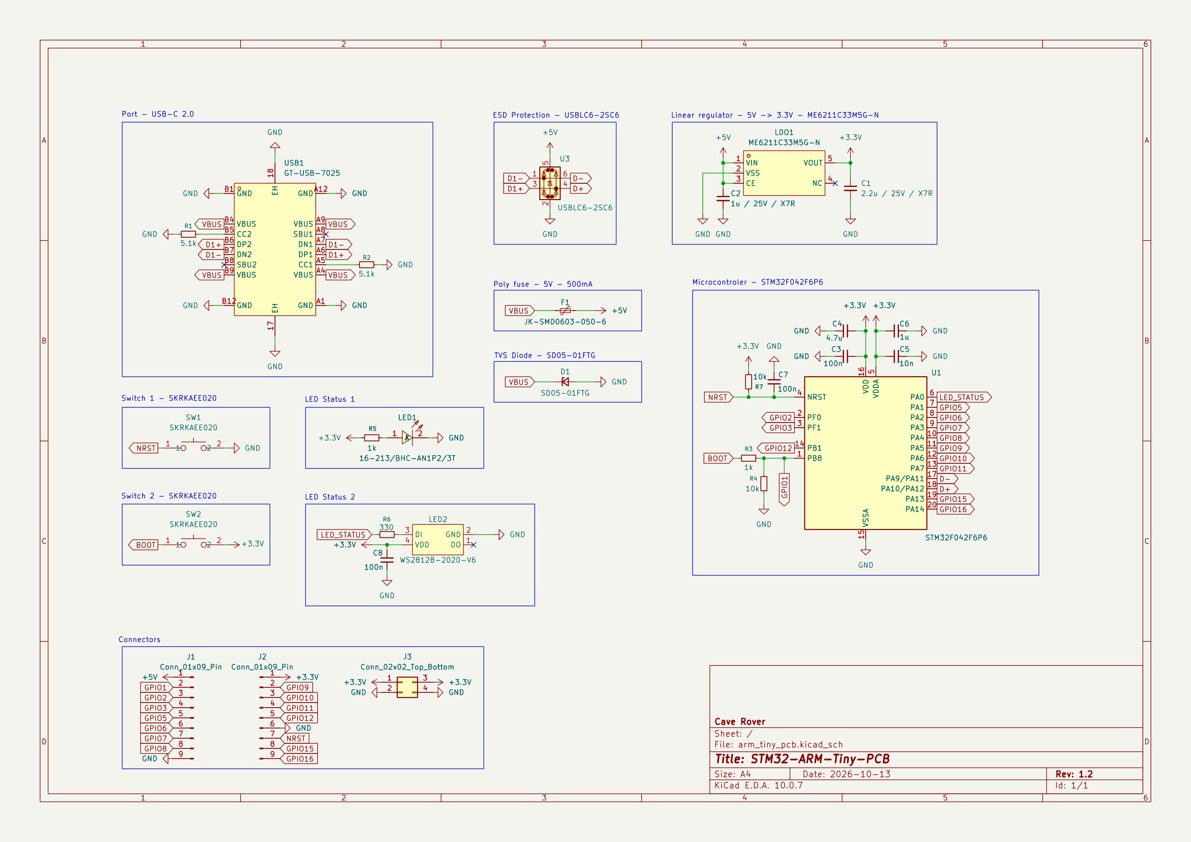
🔎 Click the schematic to open the full-resolution vector PDF → arm_tiny_pcb_sch.pdf
Power & Protection
USB-C Input: Standard Type-C receptacle (GT-USB-7025) with dual 5.1 kΩ pull-downs on CC1/CC2 for universal charger and PC host compatibility.
TVS Diode (SD05-01FTG, D1): Clamps ESD and surge events on VBUS (5 V) before they can reach the rest of the board.
Polyfuse (F1, 500 mA): Resettable fuse between VBUS and the 5 V rail.
USB Data Protection (USBLC6-2SC6, U3): Low-capacitance ESD protection on D+ / D-, preserving Full-Speed signal integrity.
LDO Regulator (ME6211C33M5G-N, LDO1): 5 V → 3.3 V, low dropout and very low quiescent current.
Ceramic-Only Capacitors: Tantalum capacitors were replaced by X7R ceramic capacitors (C1 2.2 µF, C2 1 µF, 25 V, 0805) around the regulator: more stable with this LDO, smaller, non-polarized, and free of tantalum failure modes (inrush / surge).
Decoupling:C3 100 nF, C4 4.7 µF, C5 10 nF and C6 1 µF placed close to the VDD / VDDA pins.
Signal Routing
Differential USB Pair: Matched $D^+$ and $D^-$ traces routed side-by-side with an unbroken ground reference plane on the bottom layer to maintain high signal integrity.
🧾 Key Components
Ref
Part
Function
U1
STM32F042F6P6
Microcontroller (TSSOP-20)
LDO1
ME6211C33M5G-N
3.3 V LDO regulator (SOT-23-5)
U3
USBLC6-2SC6
ESD protection for USB data lines
D1
SD05-01FTG
5 V TVS diode on VBUS (SOD-323)
F1
JK-SMD0603-050-6
0603 resettable fuse (500 mA)
USB1
GT-USB-7025
USB Type-C receptacle
SW1 / SW2
SKRKAEE020
RESET / BOOT tactile switches
LED1
16-213/BHC-AN1P2/3T
Red 3V3 power LED
LED2
WS2812B-2020-V6
RGB STATUS LED (addressable)
J1 / J2 / J3
1×9 / 1×9 / 2×2 pin headers
I/O and power headers
📝 Revision History
Change
Before
Now
Board size
26 mm × 36 mm
20 mm × 38.5 mm
LDO regulator
XBL1117-3.3 (SOT-89)
ME6211C33M5G-N (SOT-23-5)
Regulator capacitors
Tantalum (EIA-3528)
X7R ceramic (0805)
5 V input protection
Fuse only
Fuse + SD05-01FTG TVS diode
[blocked]
💻 Getting Started & Programming
1. Entering Native USB DFU Mode
No external probe needed:
Hold down the BOOT button.
Press and release the RESET button (or plug the USB-C cable into your PC).
Release the BOOT button.
Your computer now recognizes the device as an STM32 BOOTLOADER in DFU mode.
2. Flashing
Flash compiled .bin or .hex firmware using your tool of choice:
STM32CubeProgrammer (GUI / CLI)
dfu-util:bash
dfu-util -a 0 -d 0483:df11 --dfuse-address 0x08000000 -D firmware.bin
SWD (optional): connect an ST-Link to GND, 3V3, PA13 (SWDIO) and PA14 (SWCLK) on J1 / J2.
3. Firmware Support
STM32CubeIDE / Keil / IAR: Native C/C++ development with STM32 HAL / LL drivers.
PlatformIO & Arduino: Fully compatible via the official STM32duino Core.
Project library tables (paths relative to the project)
📦 Libraries: everything needed to open the project is included. The NanoCortex libraries are registered automatically when you open arm_tiny_pcb.kicad_pro with KiCad 10.
🎯 Roadmap & Target Application Projects
This board serves as the prototyping brain for three dedicated embedded hardware projects:
Active Op-Amp Reconstruction Filter: 2nd- or 4th-order active low-pass filter (Sallen-Key / Rauch topology) to smooth PWM into clean analog audio.
Analog Processing & Overdrive Stage: Soft-clipping diode distortion stage within the op-amp feedback loop (classic overdrive pedal architecture) with active gain control.
Active Tone Control & Output Stage: Active Baxandall bass/treble tone stack and low-impedance audio buffer for headphones or line-level output.
A hands-on power electronics project to master switch-mode power supplies (Buck converters), op-amp feedback injection, and USB Power Delivery:
Synchronous Buck Stage: Design of an external 24 V DC → 5 V–20 V / 3 A step-down converter (MOSFET selection, inductor saturation $I_{sat}$, and low-ESR ripple filtering).
Op-Amp Feedback Injection: Dynamic voltage margin/target control via active op-amp summing into the Buck controller's feedback (FB) node.
USB-PD PHY Communication (FUSB302B): I2C control of a dedicated USB-PD Source controller to negotiate 5 V, 9 V, 15 V, and 20 V profiles with laptops and phones.
Power Telemetry & Safety: Real-time $V_{out}$ / $I_{out}$ monitoring via STM32 12-bit ADC, over-current/over-voltage shutdown, and $V_{BUS}$ power-switch control.
🧪 Board Validation Milestones
KiCad 10 schematic design & 2-layer PCB layout with matched USB differential pairs.
Hardware Revision: 20 mm × 38.5 mm form factor, TVS protection diode, ME6211 LDO, and MLCC ceramic capacitors.
PCB fabrication and prototype SMD assembly.
USB DFU bootloader and crystal-less CRS clock verification.
3.3 V power rail validation (ripple, stability, and transient response under load).
🤝 Contributing & Feedback
Suggestions, questions, and PRs are very welcome! Whether you are a student exploring embedded design or an experienced engineer with layout tips, feel free to open an Issue or submit a Pull Request.
⚖️ Reciprocal Sharing: You are free to study, modify, build, and distribute this board. If you distribute modified versions or products based on this design, you must make the complete modified source files available under the same CERN-OHL-S v2 license.
It measures 20 × 38.5 mm and has 2 copper layers, 1.6 mm thick.
What parts does the Arm tiny pcb use?
29 parts, built around the STM32F042F6P6, USBLC6-2SC6, SKRKAEE020 and 16-213/BHC-AN1P2/3T. The full list of its parts is on this page, with links to each part's symbol and footprint where PCBKit's library has them.
Where can I download the Arm tiny pcb KiCad files?
From the Chicken-Fried/STM32-NanoCortex repository on GitHub, at the commit this page was made from: the board is arm_tiny_pcb.kicad_pcb and its schematic arm_tiny_pcb.kicad_sch. PCBKit opens the board in the browser, with nothing to install.
Can I use the Arm tiny pcb design in my own project?
Its repository publishes it under the CERN-OHL-S-2.0 licence: you may reuse it on that licence's terms (keep the author's notice, and for a copyleft licence share your changes alike).





 [blocked]