6 layers69.7 × 114.8 mm

 blinken/power-rail-probe101
Low-noise oscilloscope power rail probe
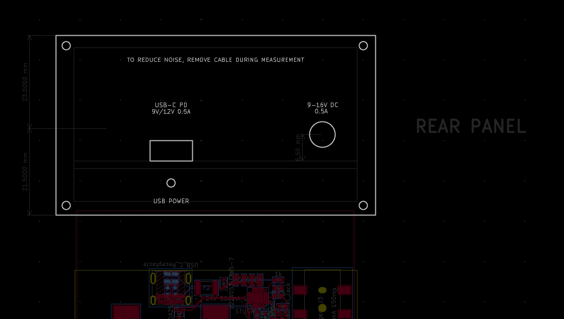
Low noise power probe panel is an open-source printed circuit board by blinken, from the blinken/power-rail-probe repository on GitHub. It is a 6-layer board of 149.4 × 124.8 mm with 245 parts on 210 nets, routed with 880 tracks and 608 vias.
It is built around the DW01A, ADP7142AUJZ-2.5-R7 and ADP7182AUJZ-2.5-R7, with the LM311DRG, LM334DT and MCP73213T-A6SI/MF among its other parts. Its parts include 78 resistors, 40 capacitors, 30 diodes, 24 ICs and 16 connectors. It belongs with the sensors and measurement boards of this library.


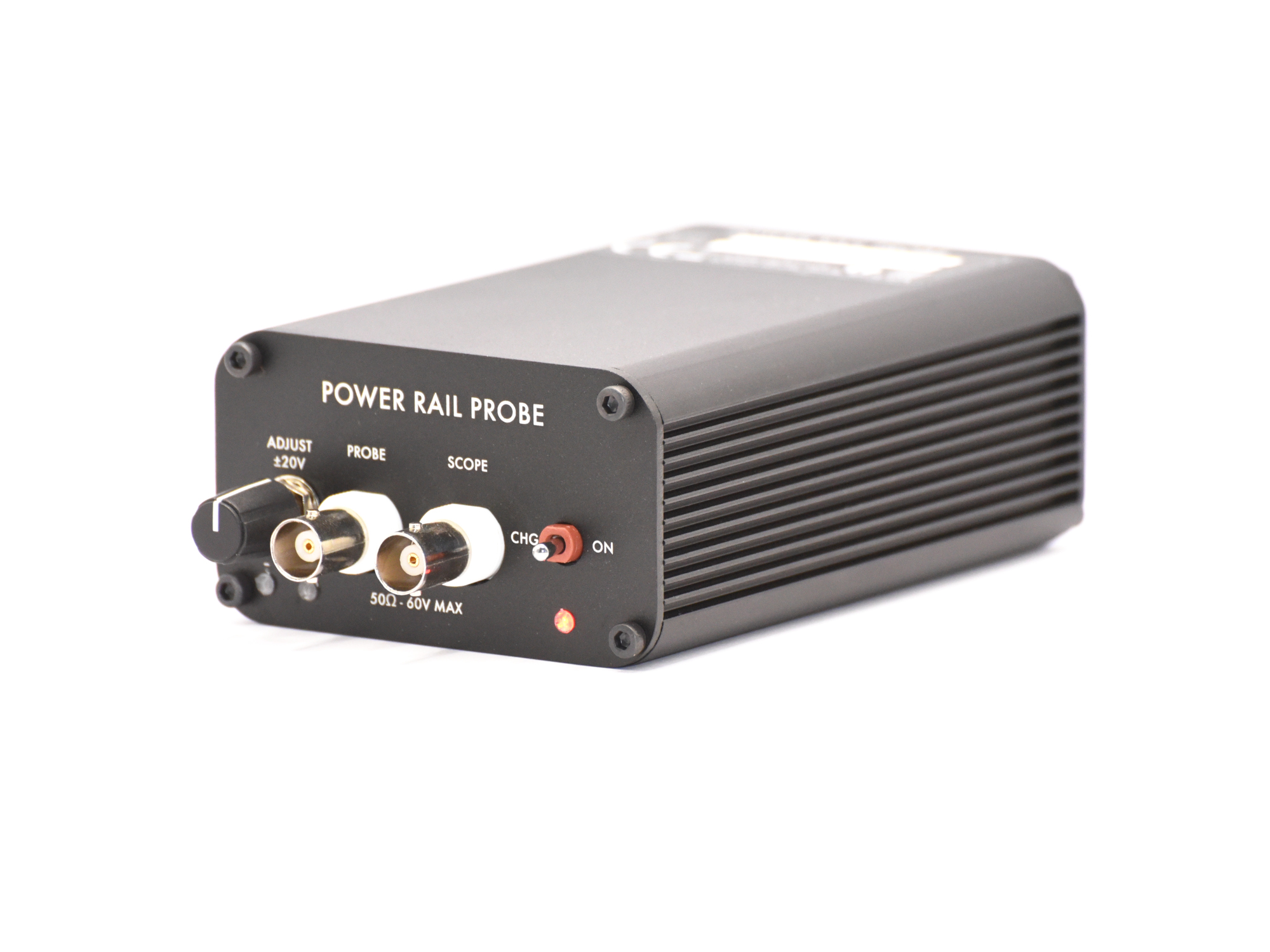
An Open Hardware low-noise power rail oscilloscope probe, loosely based on the excellent writeup by Andrew Levido [PDF archive].
The probe allows you to measure millivolt-level ripple on a power rail up to 20V, using a normal oscilloscope, by applying a vertical offset. This open design costs <10% of the price of the Tektronix TPR1000.
Here's how it works:
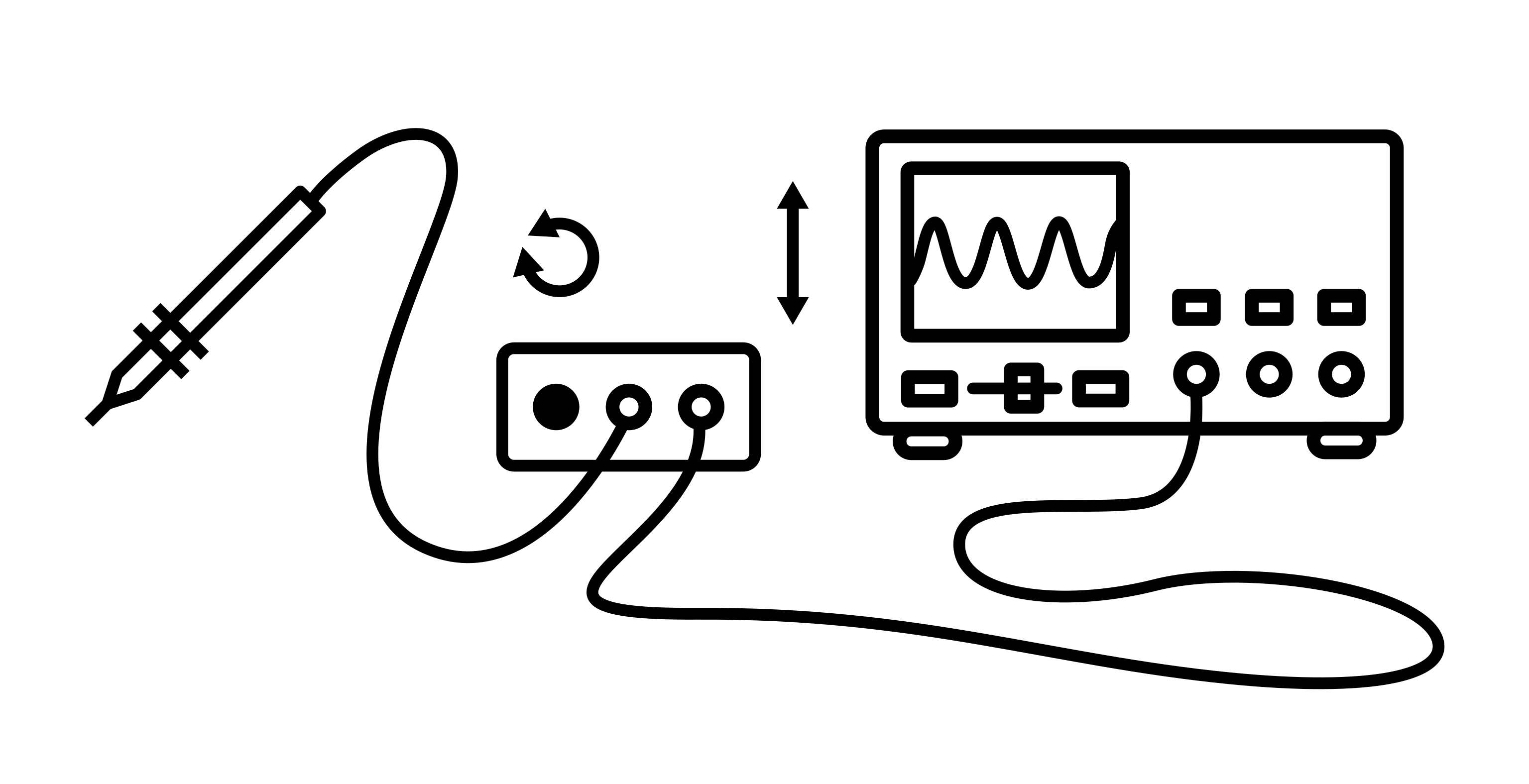
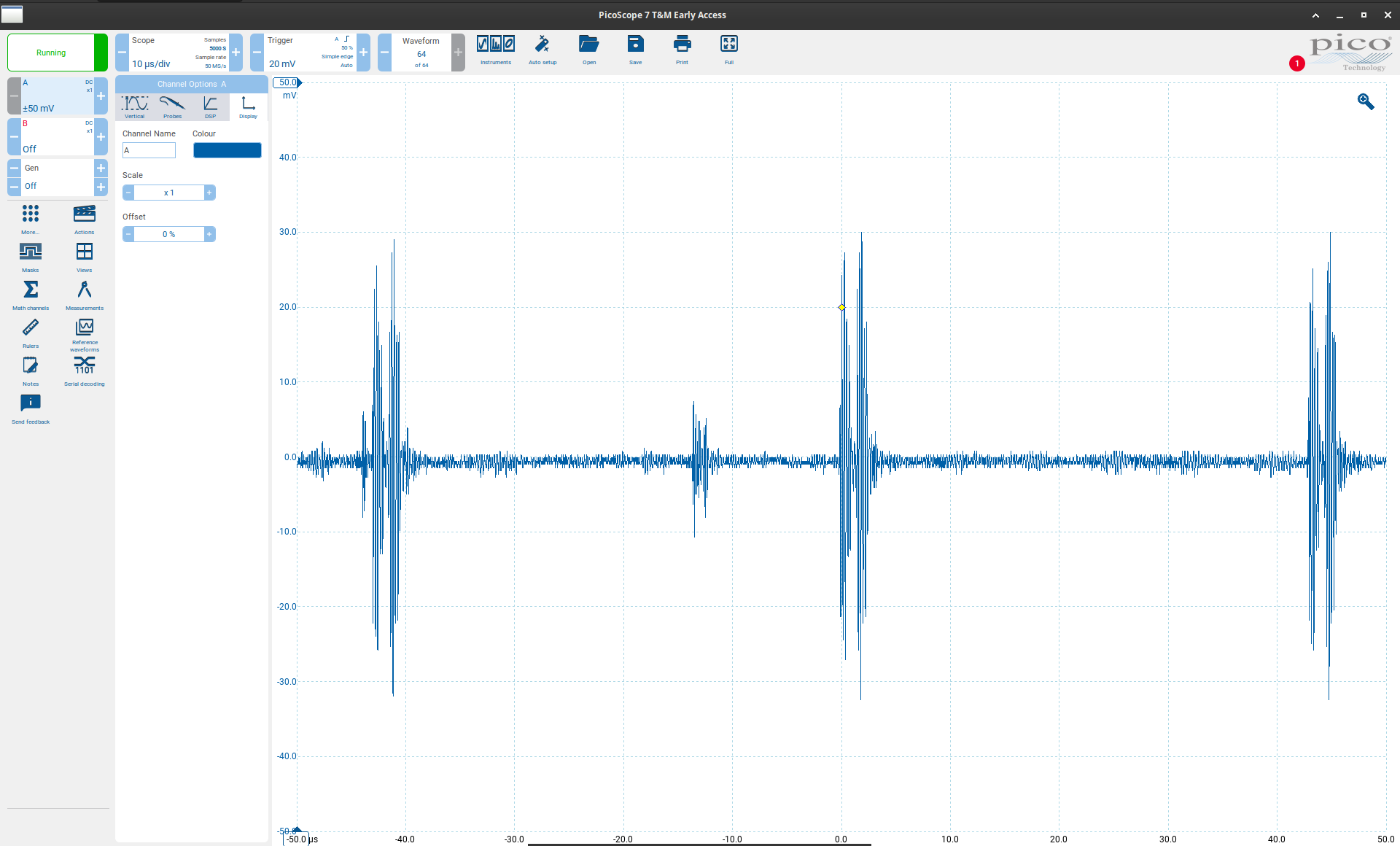
Measurement of 60mV p-p ripple on a 20V rail (ie. ripple 19.97V - 20.03V) using an inexpensive Picoscope 2204A
The probe is directly connected to a power rail you're interested in (eg, via a 1X oscilloscope probe, or a direct cable connection). AC is passed, and an adjustable offset is applied to the DC voltage. The offset is fixed, allowing DC sag and drift to be examined.
Your oscilloscope sees 0V DC, allowing power supply ripple and transients to be viewed at the 1 mV/div setting, rather than 5 V/div. It's effectively a much more powerful DC offset function for your oscilloscope.
The probe should be connected to an oscilloscope set to 50-ohm input impedance, and works best with inputs <1-ohm impedance.
Feedback and comments on the design are very much appreciated.
Version 1.0 is available to purchase fully assembled here for approx. £249 (USD $317, EUR €287). Purchasing a fully assembled unit helps to fund development!
If you would like to assemble the v1.0 probe yourself, blank PCBs, enclosures and machined front panels are also available at paradar.co.uk.
Gerber files and a full BOM & schematic are available below under a CC BY-SA 4.0 license.
The project is under active development, and there are several versions:
| Version | Status | Description | Performance |
|---|---|---|---|
| v1.0 | Completed | Initial proof-of-concept | Functions well. Frequency response flat within 1.3dB to 500MHz. Similar (or slightly better) noise levels vs v1.1 |
| v1.0.1 | Complete, characterised and available | Fix bugs from 1.0 and improve manufacturability | Improved frequency response vs v1.0, plus indicators for over/under range |
| v1.1 | Simulation complete | Includes additional compensation & lessons learned from v1.0 | Untested. Frequency response estimated from simulation as flat to within 0.5dB to 1GHz |
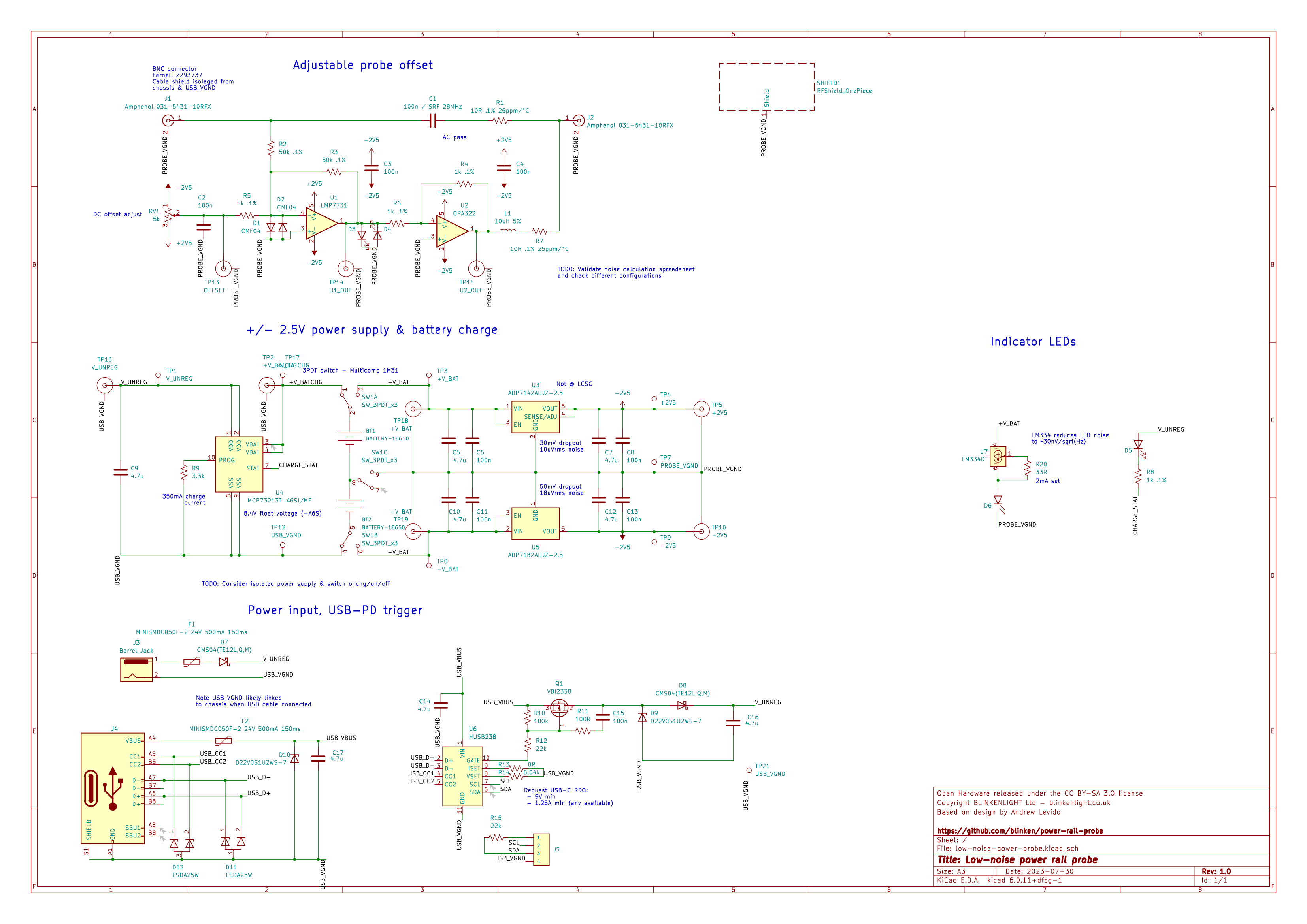
[KiCanvas]
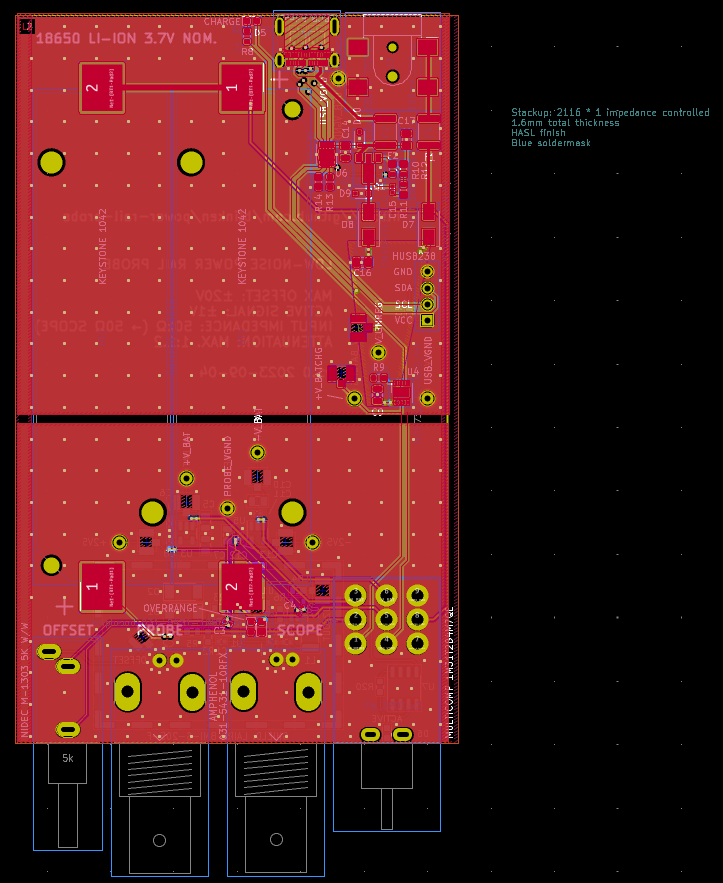
This version is under active development.
[KiCanvas]
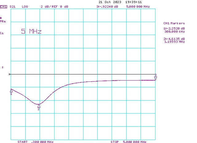
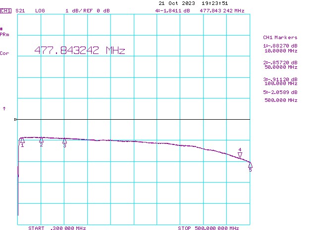
The probe's frequency response is flat within 1dB between approximately 3MHz and 490MHz, and flat within 2.5dB between approximately 150kHz and 550Mhz.
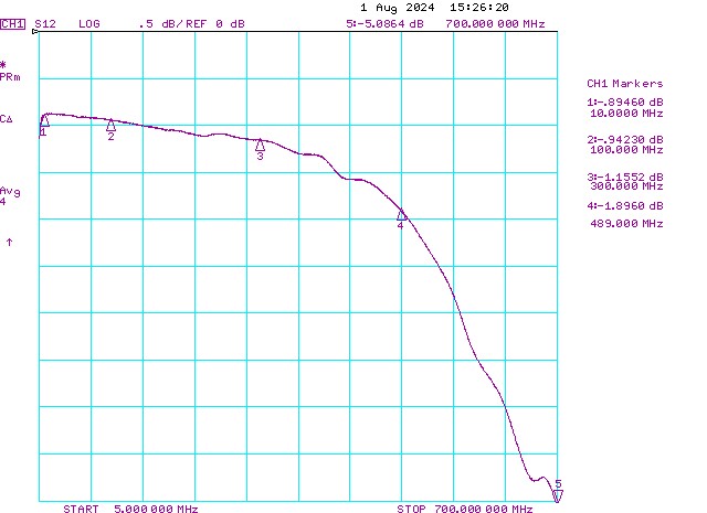
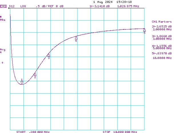
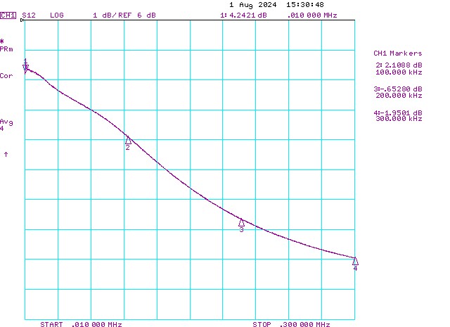
Performance is flat within 1.3dB to 500MHz, aside from a 3.7dB dip at approx 1.2MHz.
This version has not yet been manufactured, and the results below are from simulation in SPICE.
Frequency response is flat within 0.5dB to 1GHz, with the exception of a 2.5dB peak at 71.8kHz.
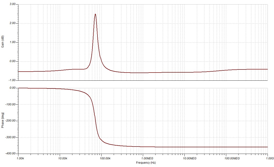
The chart above was obtained through simulation with TINA-TI SPICE, assuming an input impedance of 0.1Ω. Measuring the frequency response with a 50Ω source (ie. a standard VNA) will produce different results.
The design aims to minimise the noise introduced by the instrument. Low-noise operation is achieved with battery operation, and by avoiding semiconductors in the critical path. Batteries are recharged when the instrument is turned off.
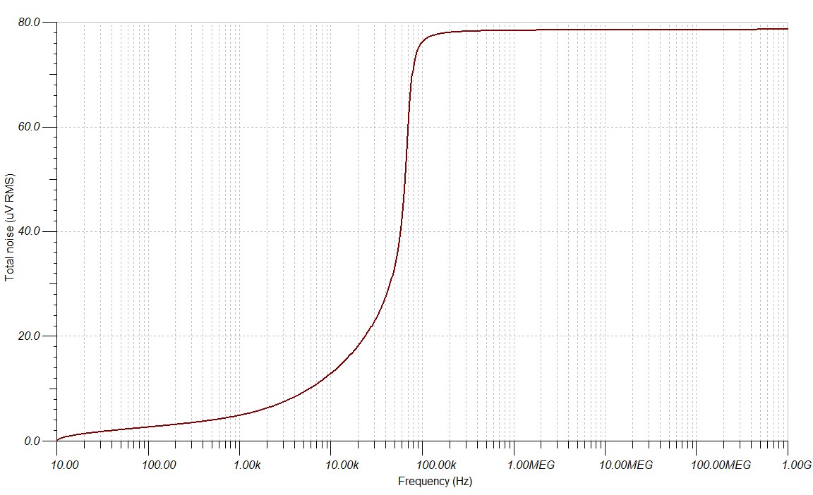
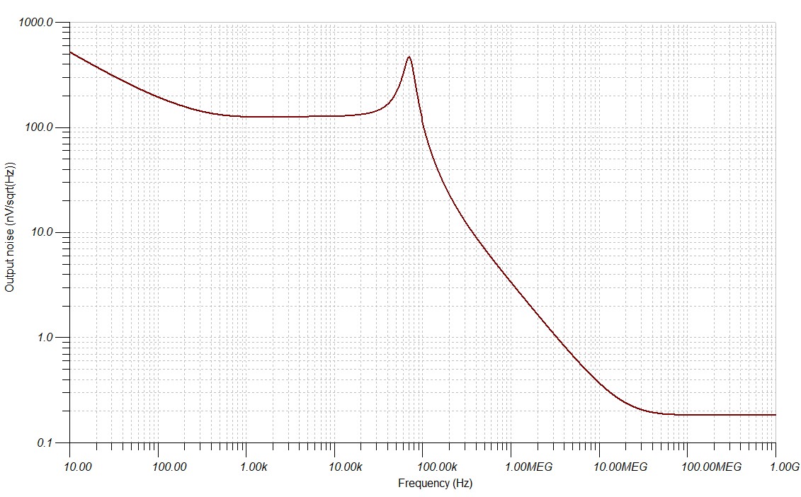
The total noise introduced by the probe (simulated in TINA-TI SPICE v9) is 78.7 µVrms when measuring over the total instrument bandwidth 10Hz and 1GHz.
The noise introduced depends on the bandwidth of the measurement. Reducing the measured bandwidth will reduce the noise introduced, and so the numbers below are a worst-case upper limit. For example, a measurement between 10kHz and 20kHz, the probe will introduce 12.9 µVrms noise (-84.8 dBm).
| Measurement bandwidth | Total RMS noise | Total peak-to-peak noise (6σ) | Power (Z0=50Ω) |
|---|---|---|---|
| 10Hz - 10kHz | 12.9 µVrms | 77.4 µVp-p | -84.8 dBm |
| 1kHz - 10kHz | 11.9 µVrms | 71.4 µVp-p | -85.5 dBm |
| 10Hz - 100kHz | 76.3 µVrms | 457.8 µVp-p | -69.3 dBm |
| 10Hz - 1MHz | 78.4 µVrms | 470.4 µVp-p | -69.1 dBm |
| 10Hz - 10MHz | 78.5 µVrms | 471.0 µVp-p | -69.1 dBm |
| 10Hz - 100MHz | 78.5 µVrms | 471.0 µVp-p | -69.1 dBm |
| 10Hz - 1GHz | 78.7 µVrms | 472.2 µVp-p | -69.1 dBm |
[CSV]
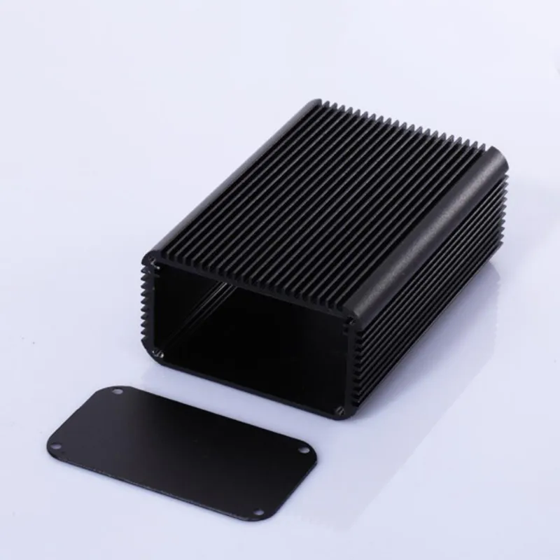
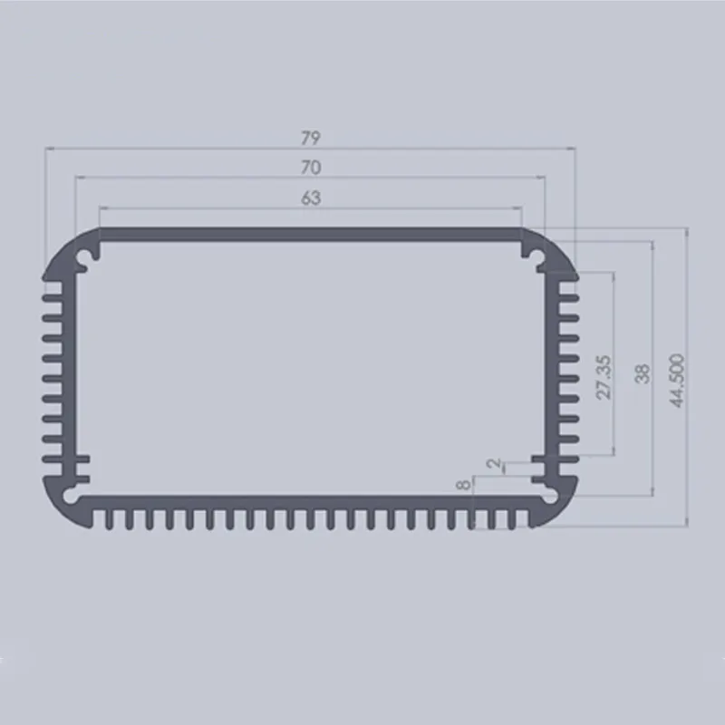
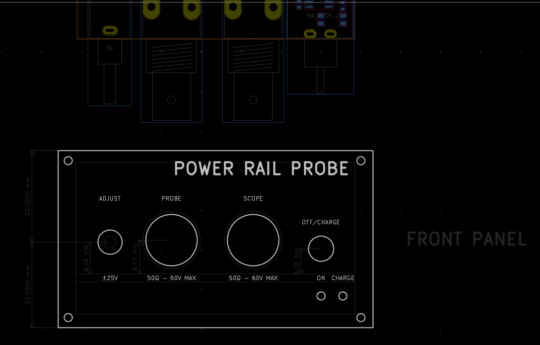
A blank PCB, aluminium extrusion case and machined front/rear panels can be purchased as a kit from paradar.co.uk.
Click to expand.
| Qty | Value | Footprint | References |
|---|---|---|---|
| 34 | 2.2u | Capacitor_SMD:C_0402_1005Metric | C2, C2, C10, C10, C11, C11, C12, C12, C13, C13, C15, C15, C19, C19, C21, C21 +18 |
| 14 | SD24-MS | misc:D_SOD-323_silkpolarity | D9, D9, D10, D10, D11, D11, D12, D12, D13, D13, D14, D14, D15, D15 |
| 12 | 10R 200mW | Resistor_SMD:R_0603_1608Metric | R11, R11, R27, R27, R28, R28, R29, R29, R30, R30, R32, R32 |
| 12 | HL2312 | Package_TO_SOT_SMD:SOT-23 | Q2, Q2, Q3, Q3, Q4, Q4, Q5, Q5, Q6, Q6, Q7, Q7 |
| 10 | 1k | Resistor_SMD:R_0603_1608Metric | R8, R8, R21, R21, R23, R23, R33, R33, R35, R35 |
| 10 | Red 1.8V | misc:LED_0603_1608Metric_polaritysilk | D1, D1, D3, D3, D4, D4, D5, D5, D6, D6 |
| 8 | 100R | Resistor_SMD:R_0603_1608Metric | R31, R31, R36, R36, R37, R37, R39, R39 |
| 8 | RF Shield Clip | misc:ICSRC6508-015SFR | J8, J8, J9, J9, J11, J11, J12, J12 |
| 8 | SMD1206-050C-24V | Fuse:Fuse_1206_3216Metric | F1, F1, F2, F2, F3, F3, F4, F4 |
| 6 | 1k .1% | Resistor_SMD:R_0603_1608Metric | R6, R6, R25, R25, R34, R34 |
| 6 | 50k | Resistor_SMD:R_0603_1608Metric | R10, R10, R22, R22, R24, R24 |
| 6 | Fiducial | Fiducial | KiKit_FID_B_1, KiKit_FID_B_2, KiKit_FID_B_3, KiKit_FID_T_1, KiKit_FID_T_2, KiKit_FID_T_3 |
| 4 | 0R | Resistor_SMD:R_0603_1608Metric | R13, R13, R26, R26 |
| 4 | 10uF | Capacitor_SMD:C_0805_2012Metric | C9, C9, C14, C14 |
| 4 | 1N5819WS | Diode_SMD:D_SOD-323 | D7, D7, D8, D8 |
| 4 | 50k .1% | Resistor_SMD:R_0603_1608Metric | R2, R2, R3, R3 |
| 4 | 5k | Resistor_SMD:R_0603_1608Metric | R9, R9, R38, R38 |
| 4 | 6.04k | Resistor_SMD:R_0603_1608Metric | R12, R12, R14, R14 |
| 4 | 620 | Resistor_SMD:R_0603_1608Metric | R16, R16, R17, R17 |
| 4 | Amphenol 901-10138 | rf-connectors:SMA_Amphenol_901-10138_Horizontal | J1, J1, J2, J2 |
| 4 | DNP | Resistor_SMD:R_0603_1608Metric | R18, R18, R19, R19 |
| 4 | DW01A | Package_TO_SOT_SMD:SOT-23-6 | U11, U11, U12, U12 |
| 4 | HY2213 | Package_TO_SOT_SMD:SOT-23-6 | U10, U10, U13, U13 |
| 4 | MountingHole_3.2mm_M3 | MountingHole:MountingHole_3.2mm_M3 | NPTH1, NPTH1, NPTH2, NPTH2 |
| 4 | OPA354 | Package_TO_SOT_SMD:SOT-23-5 | U1, U1, U2, U2 |
| 3 | NPTH | NPTH | KiKit_TO_1, KiKit_TO_2, KiKit_TO_3 |
| 2 | +V_BAT | TestPoint:TestPoint_Pad_D2.0mm | TP3, TP3 |
| 2 | +V_BATCHG | TestPoint:TestPoint_Pad_D2.0mm | TP2, TP2 |
| 2 | -V_BAT | TestPoint:TestPoint_Pad_D2.0mm | TP8, TP8 |
| 2 | 1.21k 1% 100ppm/°C | Resistor_SMD:R_0603_1608Metric | R4, R4 |
| 2 | 100n / SRF 28MHz | Capacitor_SMD:C_0402_1005Metric | C1, C1 |
| 2 | 10M | Resistor_SMD:R_0603_1608Metric | R15, R15 |
| 2 | 10R 1% 200ppm/°C | Resistor_SMD:R_0603_1608Metric | R7, R7 |
| 2 | 10uH 5% | Inductor_SMD:L_1812_4532Metric | L1, L1 |
| 2 | 2R2 1% 400ppm/°C | Resistor_SMD:R_0603_1608Metric | R1, R1 |
| 2 | 3.3k | Resistor_SMD:R_0603_1608Metric | R5, R5 |
| 2 | 33R | Resistor_SMD:R_0603_1608Metric | R20, R20 |
| 2 | 3V3 | Diode_SMD:D_SOD-123 | D2, D2 |
| 2 | 5k | misc:Potentiometer_Nidec_M-1303 | RV1, RV1 |
| 2 | ADP7142AUJZ-2.5 | Package_TO_SOT_SMD:TSOT-23-5 | U3, U3 |
| 2 | ADP7182AUJZ-2.5 | Package_TO_SOT_SMD:TSOT-23-5 | U5, U5 |
| 2 | DC-005 2.0 | Connector_BarrelJack:BarrelJack_Horizontal | J3, J3 |
| 2 | Dual_Battery_Cell | misc:Battery-holder-18650-MYOUNG-BH-18650-A1BJ021 | BT1, BT1 |
| 2 | HUSB238 | Package_DFN_QFN:DFN-10-1EP_3x3mm_P0.5mm_EP1.65x2.38mm | U6, U6 |
| 2 | LM311DR | Package_SO:SOIC-8_3.9x4.9mm_P1.27mm | U8, U8 |
| 2 | LM334DT | Package_SO:SO-8_3.9x4.9mm_P1.27mm | U7, U7 |
| 2 | MCP73213T-A6SI/MF | Package_DFN_QFN:DFN-10-1EP_3x3mm_P0.5mm_EP1.55x2.48mm | U4, U4 |
| 2 | PROBE_VGND | TestPoint:TestPoint_Pad_D2.0mm | TP7, TP7 |
| 2 | SW_3PDT_x3 | misc:Switch_3PDT_C&K_7301MD9ABE | SW1, SW1 |
| 2 | USB_C_Receptacle | Connector_USB:USB_C_Receptacle_Molex_105450-0101 | J4, J4 |
| 2 | USB_VGND | TestPoint:TestPoint_Pad_D2.0mm | TP12, TP12 |
| 2 | USB_VGND | TestPoint:TestPoint_Keystone_5000-5004_Miniature | TP21, TP21 |
| 2 | V_UNREG | TestPoint:TestPoint_Pad_D2.0mm | TP1, TP1 |
| 2 | WSE3099 | Package_TO_SOT_SMD:SOT-89-3 | Q1, Q1 |

Ledger-Donjon/curmea
To analyze the power consumption of a component, it is common to measure the current going to the ground by placing a small resistor and measuring the voltage across it.


es-ude/eeg-hardware
Repo of the Custom Hardware Design Files of the EEG-based Gaming Controller


amonbenson/expad
A four-jack USB MIDI adapter for expression and sustain pedals, built on a Raspberry Pi Pico 2 W. It works out what is plugged into each jack - whichever contact a pedal's wiper is on, and whether it is a potentiometer…

It measures 149.4 × 124.8 mm and has 6 copper layers, 4.69 mm thick.
245 parts, built around the DW01A, ADP7142AUJZ-2.5-R7, ADP7182AUJZ-2.5-R7 and LM311DRG. The full list of its parts is on this page, with links to each part's symbol and footprint where PCBKit's library has them.
From the blinken/power-rail-probe repository on GitHub, at the commit this page was made from: the board is low-noise-power-probe-panel.kicad_pcb and its schematic low-noise-power-probe.kicad_sch. PCBKit opens the board in the browser, with nothing to install.
Its repository states no licence, so its author keeps all rights: ask blinken before reusing the design.