2 layers53.8 × 28.5 mm
MSPMO
adityajoshi2008/MSPM0-DevKit
🌐 ARM Cortex-M0+ • KiCad 10.0 • Open Source • PCB Hardware
38 partsMIT

 basillx1/mspm0-accelerometer-board
2-layer KiCad board: TI MSPM0 MCU + LIS2DH accelerometer, USB-C, SWD debug
PCB Tutorial is an open-source printed circuit board by basillx1, from the basillx1/mspm0-accelerometer-board repository on GitHub, published under the MIT licence. It is a 2-layer board of 59.8 × 35.5 mm with 37 parts on 61 nets, routed with 315 tracks and 142 vias.
It is built around the MSPM0G3507SPTR, CH340E and LIS2DH, with the SPX3819M5-L-3-3, USB4105-GF-A and USBLC6-2SC6 among its other parts. Its parts include 14 capacitors, 8 resistors, 4 ICs, 2 connectors and 1 diode. It belongs with the sensors and measurement and interfaces and adapters boards of this library.


A 2-layer development board built around a TI MSPM0-series microcontroller with a 3-axis accelerometer, USB-C connectivity, and SWD debugging. Designed in KiCad 9.
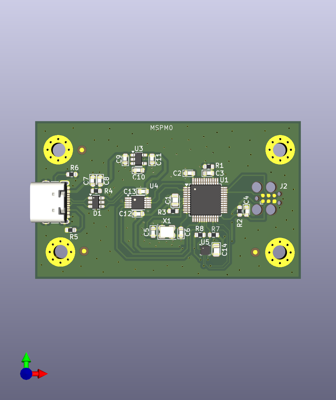
The board enumerates over USB-C and exposes the MCU's UART through an on-board USB-serial converter, reads motion data from an I2C accelerometer, and is programmed/debugged through a Tag-Connect SWD footprint (no header soldering required).
| Block | Part | Notes |
|---|---|---|
| MCU | TI MSPM0 series | 8 MHz external crystal, SWD debug |
| Accelerometer | ST LIS2DH | I2C, both interrupt lines routed to the MCU |
| USB-UART | WCH CH340E | 3.3 V operation (V3 tied to VCC) |
| USB connector | GCT USB4105 (USB-C 2.0) | Power + data |
| Regulator | 3.3 V LDO | Powers the whole board from VBUS |
| Debug | Tag-Connect TC2030 | SWD, zero-cost footprint |
gerbers/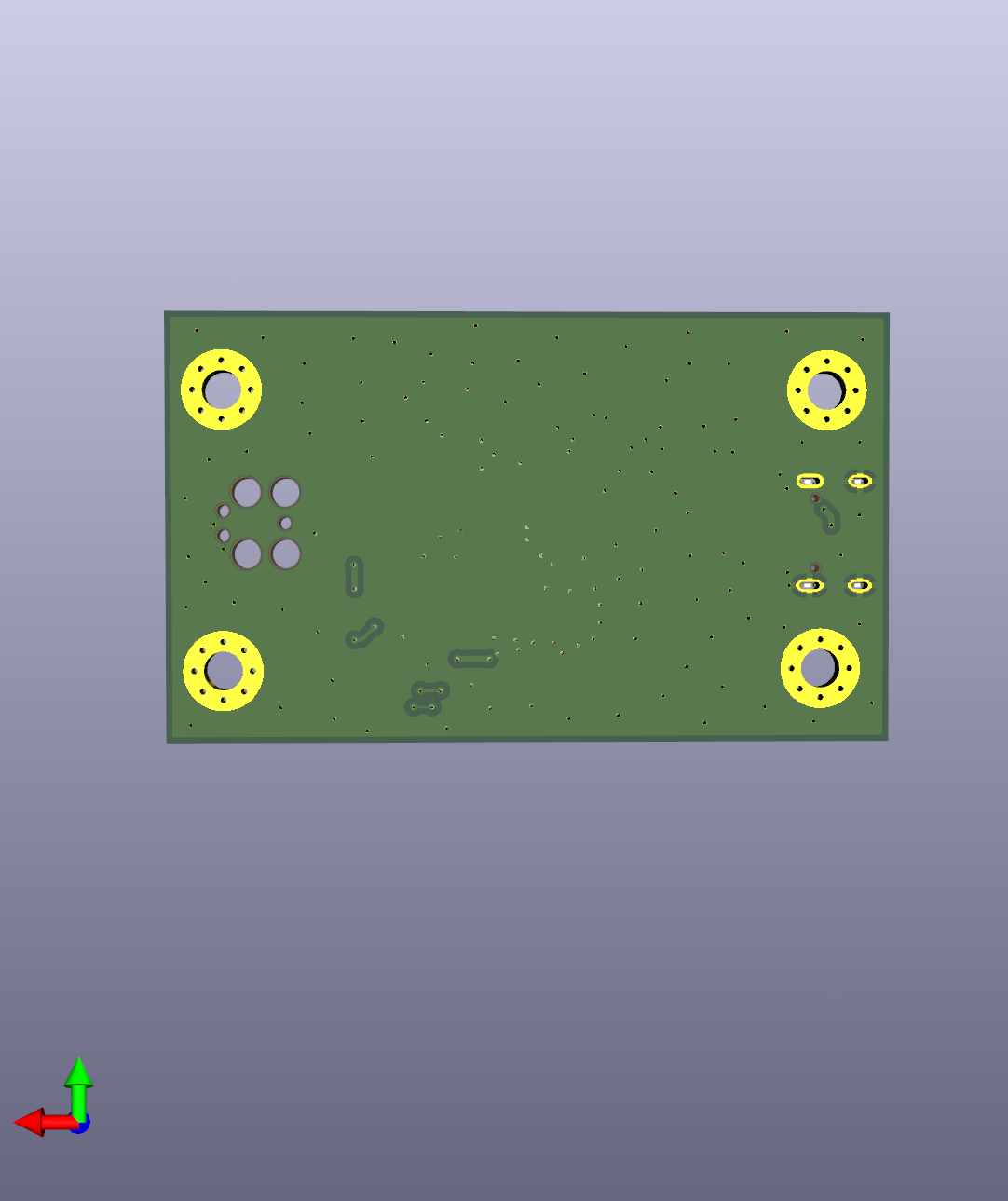
PCB-Tutorial.kicad_pro / .kicad_sch / .kicad_pcb   KiCad 9 project files
MSPM0-tutorialSchemSymbLib.kicad_sym               Custom symbol library
gerbers/                                           Fabrication outputs
board-front.png / board-back.png Board rendersThis was my first full schematic-to-fabrication PCB. Things that bit me along the way, and what fixed them:
MIT - see LICENSE. Design provided as-is; not yet validated on physical hardware.
| Qty | Value | Footprint | References |
|---|---|---|---|
| 5 | 470n | LED_SMD:LED_0603_1608Metric | C7, C8, C10, C12, C13 |
| 5 | 5k1 | Resistor_SMD:R_0603_1608Metric | R2, R5, R6, R7, R8 |
| 4 | M3 | MountingHole:MountingHole_3.2mm_M3_Pad_Via | MH1, MH2, MH3, MH4 |
| 3 | 470u | LED_SMD:LED_0603_1608Metric | C2, C3, C4 |
| 3 | Fiducial | Fiducial:Fiducial_1mm_Mask2mm | FID1, FID2, FID3 |
| 2 | 0R | Resistor_SMD:R_0603_1608Metric | R1, R4 |
| 2 | 10u | LED_SMD:LED_0603_1608Metric | C9, C11 |
| 2 | 15p | LED_SMD:LED_0603_1608Metric | C5, C6 |
| 1 | 100k | Resistor_SMD:R_0603_1608Metric | R3 |
| 1 | 10u | LED_SMD:LED_0805_2012Metric | C1 |
| 1 | 470n | LED_SMD:LED_0805_2012Metric | C14 |
| 1 | 8MHz | Crystal:Crystal_SMD_3225-4Pin_3.2x2.5mm | X1 |
| 1 | CH340E | Package_SO:MSOP-10_3x3mm_P0.5mm | U4 |
| 1 | LIS2DH | Package_LGA:LGA-14_2x2mm_P0.35mm_LayoutBorder3x4y | U5 |
| 1 | MSPM0G3507SPTR | Package_QFP:LQFP-48_7x7mm_P0.5mm | U1 |
| 1 | SPX3819M5-L-3-3 | Package_TO_SOT_SMD:SOT-23-5 | U3 |
| 1 | TC2030 | Connector:Tag-Connect_TC2030-IDC-FP_2x03_P1.27mm_Vertical | J2 |
| 1 | USB4105-GF-A | Connector_USB:USB_C_Receptacle_GCT_USB4105-xx-A_16P_TopMnt_Horizontal | J1 |
| 1 | USBLC6-2SC6 | Package_TO_SOT_SMD:SOT-23-6 | D1 |
It measures 59.8 × 35.5 mm and has 2 copper layers, 1.6 mm thick.
37 parts, built around the MSPM0G3507SPTR, CH340E, LIS2DH and SPX3819M5-L-3-3. The full list of its parts is on this page, with links to each part's symbol and footprint where PCBKit's library has them.
From the basillx1/mspm0-accelerometer-board repository on GitHub, at the commit this page was made from: the board is PCB-Tutorial.kicad_pcb and its schematic PCB-Tutorial.kicad_sch. PCBKit opens the board in the browser, with nothing to install.
Its repository publishes it under the MIT licence: you may reuse it on that licence's terms (keep the author's notice, and for a copyleft licence share your changes alike).
adityajoshi2008/MSPM0-DevKit
🌐 ARM Cortex-M0+ • KiCad 10.0 • Open Source • PCB Hardware

benbruder/MSPM0
Design of schematic and PCB for a TI MSPM0-based MCU with all of its components.

MikhalevDima/MSPM0-TutorialPCB
Учебный проект, двухслойной печатной платы. Спроектированная в KiCad.

ctrl-z3d/pcb-designs
A personal archive of PCB projects I've designed and built along the way. Schematics, board layouts, manufacturing files, and notes.

hykoser/LIS2DH-Accelerometer-Board
A custom accelerometer development board designed with KiCad and MSPM0 microcontroller.

prashantbhandary/mspmo-baord
A compact USB-C development board for TI's MSPM0G3507 (Arm Cortex-M0+, 80 MHz, 128 KB flash, 32 KB SRAM), with an on-board USB-to-UART bridge, a 3-axis accelerometer and a Tag-Connect SWD footprint.

