
4 layers58 × 31 mm

 ashfaque-ur-rahman/STM32WB-RF-PCB-Design
STM32 microcontroller PCB design with RF capability —4 layer Board —KiCad project based on Phil's Lab tutorial series
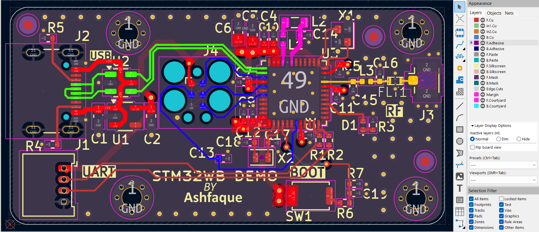
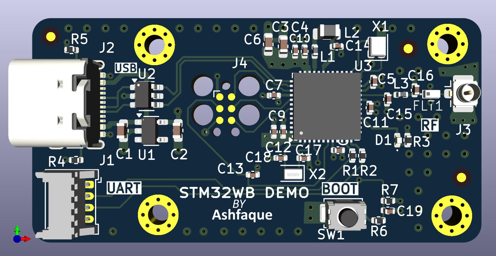
STM32 2nd Project is an open-source printed circuit board by ashfaque-ur-rahman, from the ashfaque-ur-rahman/STM32WB-RF-PCB-Design repository on GitHub. It is a 4-layer board of 48.5 × 24.3 mm with 48 parts on 55 nets, routed with 328 tracks and 102 vias.
It is built around the DLF162500LT-5028A1, MIC5365-3.3YD5-TR and USBLC6-2SC6. Its parts include 19 capacitors, 7 resistors, 4 connectors, 3 ICs and 3 inductors. It belongs with the radio and wireless boards and the STM32 boards of this library.


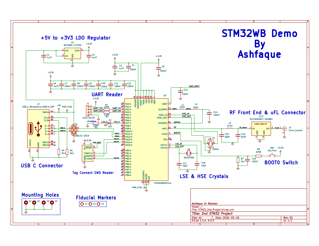
My second STM32 PCB design, following the Phil's Lab STM32WB tutorial series. This was a significant step up from my first project — a 4-layer stackup with RF design considerations for the STM32WB55, which integrates a 2.4GHz radio for Bluetooth 5.0 and IEEE 802.15.4 (Zigbee/Thread). My first experience working with RF PCB design.
| Property | Details |
|---|---|
| MCU | STM32WB55 — UFQFPN48 package |
| Wireless | Bluetooth 5.0 / IEEE 802.15.4 (integrated 2.4GHz radio) |
| RF Filter | DLF162500LT-5028A1 — 2.4GHz balun & RF filter |
| Main crystal | ABM11 — 32.000MHz (HSE) |
| RTC crystal | ABS06 — 32.768kHz (LSE) |
| Board layers | 4-layer stackup |
| EDA Tool | KiCad |
| Design reference | Phil's Lab — STM32WB PCB Design Series |
| Status | Design complete — Gerbers exported |
This is a 4-layer PCB — a significant upgrade from standard 2-layer designs:
| Layer | Function |
|---|---|
| Layer 1 (Top) | Signal + components |
| Layer 2 | Ground plane (GND) |
| Layer 3 | Power plane (VCC) |
| Layer 4 (Bottom) | Signal |
The dedicated ground plane on Layer 2 is critical for RF performance — it provides a low-impedance return path and shields the RF traces from noise.
| Component | Part | Function |
|---|---|---|
| MCU | STM32WB55 (UFQFPN48) | Dual-core: Cortex-M4 (app) + Cortex-M0+ (RF stack) |
| RF Filter | DLF162500LT-5028A1 | 2.4GHz balun + low-pass filter for antenna matching |
| HSE Crystal | ABM11 32.000MHz | High-speed external clock |
| LSE Crystal | ABS06 32.768kHz | Low-speed RTC clock |
| File | Description |
|---|---|
STM32_2nd_Project.kicad_pro | KiCad project file |
STM32_2nd_Project.kicad_sch | Schematic |
STM32_2nd_Project.kicad_pcb | PCB layout |
RF_Filter_Library.kicad_sym | Custom RF filter symbol library |
DLF162500LT-5028A1.kicad_mod | Custom RF filter footprint |
| File | Description |
|---|---|
STM32_1st_Project-F_Cu.gbr | Front copper layer |
STM32_1st_Project-B_Cu.gbr | Back copper layer |
STM32_1st_Project-F/B_Mask.gbr | Solder mask layers |
STM32_1st_Project-F/B_Paste.gbr | Solder paste layers |
STM32_1st_Project-F/B_Silkscreen.gbr | Silkscreen layers |
STM32_1st_Project-Edge_Cuts.gbr | Board outline |
STM32_1st_Project-PTH/NPTH.drl | Drill files |
| File | Description |
|---|---|
STM32_2nd_Project_BOM.csv | Bill of materials |
STM32_2nd_Project.csv | Component placement data |
STM32_1st_Project-top/bottom-pos.csv | Pick and place files |
| File | Description |
|---|---|
UFQFPN48_A0B9_STM.step | STM32WB55 3D model |
ABM11-32.000MHZ-B7G-T.step | HSE crystal 3D model |
ABS06-32.768KHZ-T.step | LSE crystal 3D model |
DLF162500LT-5028A1.step | RF filter 3D model |

This design follows the Phil's Lab STM32WB PCB Design tutorial series.
Phil's Lab: https://www.youtube.com/@PhilsLab
Mymensingh Engineering College — EEE Department
| Qty | Value | Footprint | References |
|---|---|---|---|
| 11 | 100nF | Capacitor_SMD:C_0402_1005Metric | C4, C5, C7, C8, C9, C10, C11, C12, C13, C14, C19 |
| 4 | 220R | Resistor_SMD:R_0402_1005Metric | R1, R2, R3, R6 |
| 4 | 4u7F | Capacitor_SMD:C_0603_1608Metric | C1, C2, C3, C6 |
| 4 | MountingHole_Pad | MountingHole:MountingHole_2.2mm_M2_Pad_Via | H1, H2, H3, H4 |
| 3 | Fiducial | Fiducial:Fiducial_1mm_Mask2mm | F1, F2, F3 |
| 2 | 10pF | Capacitor_SMD:C_0402_1005Metric | C17, C18 |
| 2 | 5K1 | Resistor_SMD:R_0402_1005Metric | R4, R5 |
| 1 | 0p3F | Capacitor_SMD:C_0402_1005Metric | C16 |
| 1 | 0p8F | Capacitor_SMD:C_0402_1005Metric | C15 |
| 1 | 10nH | Inductor_SMD:L_0402_1005Metric | L1 |
| 1 | 10uH | Inductor_SMD:L_0805_2012Metric | L2 |
| 1 | 2n7H | Inductor_SMD:L_0402_1005Metric | L3 |
| 1 | 32MHz | Crystal:Crystal_SMD_2016-4Pin_2.0x1.6mm | X1 |
| 1 | 32kHz768 | Crystal:Crystal_SMD_2012-2Pin_2.0x1.2mm | X2 |
| 1 | 5k1 | Resistor_SMD:R_0402_1005Metric | R7 |
| 1 | Conn_01x04 | Connector_Molex:Molex_PicoBlade_53048-0410_1x04_P1.25mm_Horizontal | J1 |
| 1 | Conn_ARM_SWD_TagConnect_TC2030 | Connector:Tag-Connect_TC2030-IDC-FP_2x03_P1.27mm_Vertical | J4 |
| 1 | Conn_Coaxial | Connector_Coaxial:U.FL_Hirose_U.FL-R-SMT-1_Vertical | J3 |
| 1 | DLF162500LT-5028A1 | footprint:DLF162500LT-5028A1 | FLT1 |
| 1 | LED | LED_SMD:LED_0402_1005Metric | D1 |
| 1 | MIC5365-3.3YD5 | Package_TO_SOT_SMD:TSOT-23-5 | U1 |
| 1 | STM32WB55CEUx | Package_DFN_QFN:QFN-48-1EP_7x7mm_P0.5mm_EP5.6x5.6mm | U3 |
| 1 | SW_Push | Button_Switch_SMD:SW_Push_SPST_NO_Alps_SKRK | SW1 |
| 1 | USBLC6-2SC6 | Package_TO_SOT_SMD:SOT-23-6 | U2 |
| 1 | USB_C_Receptacle_USB2.0_16P | Connector_USB:USB_C_Receptacle_GCT_USB4105-xx-A_16P_TopMnt_Horizontal | J2 |


OdaiJ/stm32-bt-board
My attempt at following the Phil's Lab KiCad V7 tutorial on YouTube

shivamtiwari020505/stm32wb55-ble-dev-board
Custom STM32WB55 development board integrating 2.4GHz BLE 5.x, LPUART, I2C, and UART via RS232/DB9 for PC and industrial machine interfacing. Designed to bridge modern wireless IoT with legacy wired systems.


arsovskiteodor/A.ProdDeck
Open-hardware macro pad (WIP): custom KiCad PCB with keys, encoders and a fader, plus firmware and a desktop configurator

Bobev64/sensor-board
KiCAD design attempt at a flight controller for an RC airplane.

It measures 48.5 × 24.3 mm and has 4 copper layers, 1.58 mm thick.
48 parts, built around the DLF162500LT-5028A1, MIC5365-3.3YD5-TR and USBLC6-2SC6. The full list of its parts is on this page, with links to each part's symbol and footprint where PCBKit's library has them.
From the ashfaque-ur-rahman/STM32WB-RF-PCB-Design repository on GitHub, at the commit this page was made from: the board is STM32_2nd_Project.kicad_pcb and its schematic STM32_2nd_Project.kicad_sch. PCBKit opens the board in the browser, with nothing to install.
Its repository states no licence, so its author keeps all rights: ask ashfaque-ur-rahman before reusing the design.