2 layers190 × 144.3 mm
Amplifier
oselcukyatagan/CLASS_AB_AUDIO_POWER_AMP
This is the repository for the developing of the class AB audio power amplifier device.
85 parts

 alpnak/Analog_Common_Emitter_Amplifier
4-Stage analog common emitter amplifier design and analysis with LTspice & KiCad
211201062 Faz4 KiCad is an open-source printed circuit board by alpnak, from the alpnak/Analog_Common_Emitter_Amplifier repository on GitHub. It is a 2-layer board of 68 × 87.5 mm with 46 parts on 29 nets, routed with 321 tracks and 30 vias.
It is built around the BC546, BD139 and BD140. Its parts include 22 resistors, 3 connectors and 2 diodes. It belongs with the audio and music boards of this library.


This project details the end-to-end design of a four-stage audio amplifier, developed as part of the Analog Electronic Circuits project. The work spans theoretical mathematical analysis, detailed SPICE simulations, physical breadboard prototyping, and a final industrial-standard PCB design. By meticulously documenting the analytical computations, simulation data, and real-world test results, this repository is structured to serve as a robust, open-source foundation for upcoming theoretical electricity and electronics educational content‚ Äî specifically designed to be produced using computer graphics and text-to-speech tools rather than traditional camera recordings.
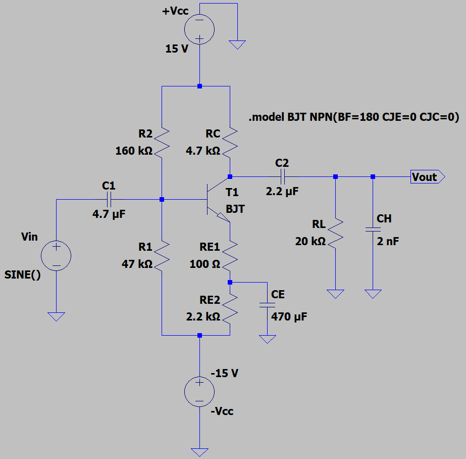
Objective: Design the foundational first gain stage of the audio amplifier using a Common Emitter configuration to provide high voltage gain.
Details: This initial phase focuses on establishing a stable DC operating point, performing AC small-signal analysis, and calculating the upper and lower cutoff frequencies for a band-pass characteristic. Utilizing ideal transistor parameters ($ eta = 180$) and a $\pm 15V$ dual supply, the stage is engineered to deliver a targeted voltage gain ($|A_v| \ge 30$) and an output voltage swing of 22-24V peak-to-peak. The design ensures the frequency response encompasses the standard audio band ($f_L \le 20 ext{ Hz}$, $f_H \ge 20 ext{ kHz}$) and is thoroughly verified through LTspice simulations (.op, .ac, .tran).
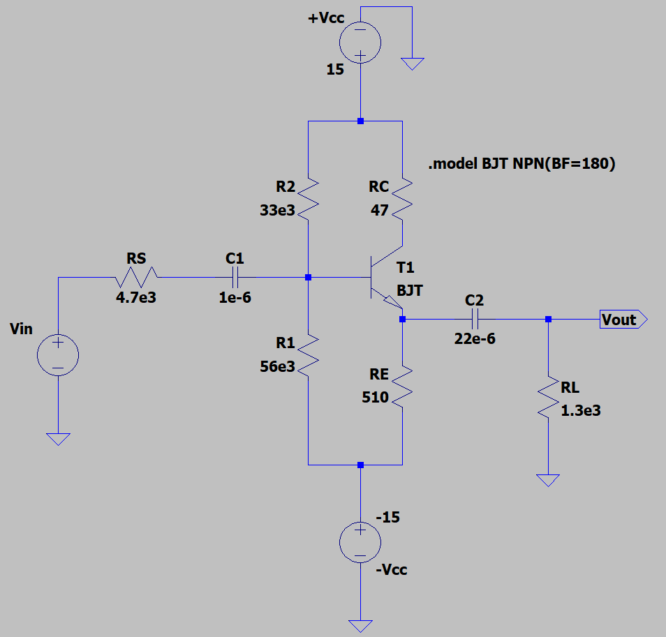
Objective: Introduce an Emitter Follower (buffer) stage to prevent loading effects between stages and successfully transition into a multistage cascaded architecture. Details: To meet higher amplification requirements, the system is expanded by cascading two Common Emitter stages followed by an Emitter Follower stage. This configuration acts as a buffer, ensuring proper impedance matching and preserving the signal integrity across stages. The selection of appropriate inter-stage coupling capacitors is critical here to maintain the 20 Hz - 20 kHz audio band requirements. The combined multistage system is designed to achieve a total voltage gain of $A_v \ge 200$ and a maximum output swing exceeding 20V peak-to-peak, all while maintaining strict power dissipation limits for each resistor ($< 0.2W$).
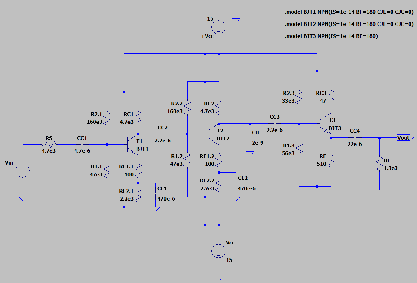
Objective: Design a Class AB push-pull output stage capable of driving an $8 \Omega$ speaker load, transition from ideal SPICE models to real-world commercial BJTs, and finalize the complete 4-stage architecture. Details: The final system architecture consists of two CE gain stages, one EF buffer stage, and a Class AB power output stage. This phase involves extensive datasheet analysis to replace the initial ideal transistors with physical components that meet the required thermal stability, current capacity, and gain bandwidth products. The Class AB stage utilizes a complementary push-pull pair with diode biasing to eliminate crossover distortion. The finalized full system targets a total voltage gain of $> 1000$ and an output power of $\ge 2 ext{W}$ over the $8 \Omega$ load, while keeping total system power consumption under 10W.
Components Selected in this Phase:
BC546B (Chosen for high $V_{CEO}$ breakdown voltage and stable current gain).BD139-16 (Selected for its thermal stability and medium-power endurance).BD139 (NPN) & BD140 (PNP) complementary pair.1N4148 fast-switching diodes.Objective: Validate the theoretical and simulated designs in the physical world and convert the validated circuit into a professional printed circuit board (PCB). Details: The complete amplifier is prototyped on a breadboard to assess real-world performance against parasitic effects, thermal drift, and component tolerances. Key metrics, including DC offset, signal gain, output power, and frequency response, are physically measured using an oscilloscope and multimeter. Following successful breadboard validation, a 2-layer (Top & Bottom) PCB layout is designed using KiCad EDA. The PCB design adheres to strict design rules, incorporating minimum trace widths for power (1 mm) and signal lines (0.3 mm), as well as dedicated thermal relief (heat sink) zones for the power transistors, ensuring a zero-error Design Rules Check (DRC).
| Qty | Value | Footprint | References |
|---|---|---|---|
| 6 | 4.7e3 | Resistor_THT:R_Axial_DIN0414_L11.9mm_D4.5mm_P15.24mm_Horizontal | R2.1 - 4.7 kΩ, R2.4 - 4.7 kΩ, RC1 - 4.7 kΩ, RC2 - 4.7 kΩ, RC3 - 4.7 kΩ, RS1 - 4.7 kΩ |
| 6 | 47e3 | Resistor_THT:R_Axial_DIN0207_L6.3mm_D2.5mm_P10.16mm_Horizontal | R1.1 - 47 kΩ, R1.2 - 47 kΩ, R2.1.1 - 47 kΩ, R2.1.2 - 47 kΩ, R2.1.7 - 47 kΩ, R2.1.8 - 47 kΩ |
| 5 | 33e3 | Resistor_THT:R_Axial_DIN0207_L6.3mm_D2.5mm_P10.16mm_Horizontal | R2.1.3 - 33 kΩ, R2.1.4 - 33 kΩ, R2.1.5 - 33 kΩ, R2.1.6 - 33 kΩ, R2.3 - 33 kΩ |
| 4 | 2.2e3 | Resistor_THT:R_Axial_DIN0414_L11.9mm_D4.5mm_P15.24mm_Horizontal | R2.2 - 2.2 kΩ, R2.5 - 2.2 kΩ, RE2.1 - 2.2 kΩ, RE2.2 - 2.2 kΩ |
| 2 | 1 | Resistor_THT:R_Axial_Power_L25.0mm_W9.0mm_P27.94mm | RE4.1 - 1 Ω, RE4.2 - 1 Ω |
| 2 | 1N4148 | Diode_THT:D_DO-35_SOD27_P7.62mm_Horizontal | D1 - 1N4148, D2 - 1N4148 |
| 2 | 2.2e-6 | Capacitor_THT:CP_Radial_D4.0mm_P2.00mm | CC2 - 2.2 μF, CC3 - 2.2 μF |
| 2 | 47 | Resistor_THT:R_Axial_DIN0207_L6.3mm_D2.5mm_P10.16mm_Horizontal | RE1.1 - 47 Ω, RE1.2 - 47 Ω |
| 2 | 470e-6 | Capacitor_THT:CP_Radial_D10.0mm_P5.00mm | CE1 - 470 μF, CE2 - 470 μF |
| 2 | BC546 | Package_TO_SOT_THT:TO-92_Inline | T1/BC546, T2/BC546 |
| 2 | BD139 | Package_TO_SOT_THT:TO-126-3_Vertical | T3, T4 |
| 2 | Conn_01x02 | Connector_PinHeader_2.54mm:PinHeader_1x02_P2.54mm_Vertical | J1, J2 |
| 1 | 100e-6 | Capacitor_THT:CP_Radial_D6.3mm_P2.50mm | CC4 - 100 μF |
| 1 | 2e-9 | Capacitor_THT:C_Disc_D7.5mm_W5.0mm_P7.50mm | CH1 - 2.2 nF |
| 1 | 39 | Resistor_THT:R_Axial_DIN0414_L11.9mm_D4.5mm_P15.24mm_Horizontal | RE3.2 - 39 Ω |
| 1 | 4.7e-6 | Capacitor_THT:CP_Radial_D5.0mm_P2.00mm | CC1 - 4.7 μF |
| 1 | 470 | Resistor_THT:R_Axial_DIN0414_L11.9mm_D4.5mm_P15.24mm_Horizontal | RE3.1 - 470 Ω |
| 1 | 56e3 | Resistor_THT:R_Axial_DIN0207_L6.3mm_D2.5mm_P10.16mm_Horizontal | R1.3 - 56 kΩ |
| 1 | 8 | Resistor_THT:R_Axial_Power_L25.0mm_W9.0mm_P27.94mm | RL1 - 8 Ω |
| 1 | BD140 | Package_TO_SOT_THT:TO-126-3_Vertical | T5 |
| 1 | Conn_01x03 | Connector_PinHeader_2.54mm:PinHeader_1x03_P2.54mm_Vertical | J3 |
oselcukyatagan/CLASS_AB_AUDIO_POWER_AMP
This is the repository for the developing of the class AB audio power amplifier device.

scout-cc/SkripsieProject
Designs and reports for personal final year engineering project


xtarke/automated_buggy
This shield connects microcontroller (MSP-EXP430FR2355) pins to the car's power board. Go to Power Board for more hardware information.
It measures 68 × 87.5 mm and has 2 copper layers, 1.6 mm thick.
46 parts, built around the BC546, BD139 and BD140. The full list of its parts is on this page, with links to each part's symbol and footprint where PCBKit's library has them.
From the alpnak/Analog_Common_Emitter_Amplifier repository on GitHub, at the commit this page was made from: the board is faz4/faz4/211201062_Faz4_KiCad.kicad_pcb and its schematic faz4/faz4/211201062_Faz4_KiCad.kicad_sch. PCBKit opens the board in the browser, with nothing to install.
Its repository states no licence, so its author keeps all rights: ask alpnak before reusing the design.