4 layers99 × 53.3 mm
PSLab
fossasia/pslab-hardware
PSLab Hardware Design and Schematics https://pslab.io
199 parts1.7kApache-2.0

 alexjx/avrdoper-re
AVR-Doper RE is a USB in-system programmer (ISP) for AVR microcontrollers. It is a respin of the original AVR-Doper, updated with an ATmega328P controller, a USB-C connector, selectable 5 V or 3.3 V target power, and a…
Avrdoper re is an open-source printed circuit board by alexjx, from the alexjx/avrdoper-re repository on GitHub. It is a 2-layer board of 75 × 30 mm with 42 parts on 49 nets, routed with 317 tracks and 34 vias.
It is built around the ATMEGA328-PU, 74HC126D and AMS1117-3.3, with the GRM21BR61A106KE19L and GT-USB-7010ASV among its other parts. Its parts include 18 resistors, 7 capacitors, 5 diodes, 5 connectors and 3 ICs. It belongs with the AVR (ATmega, ATtiny) boards of this library.


AVR-Doper RE is a USB in-system programmer (ISP) for AVR microcontrollers. It is a respin of the original AVR-Doper, updated with an ATmega328P controller, a USB-C connector, selectable 5 V or 3.3 V target power, and a compact 2×5 target connector.
This repository contains both the KiCad hardware design and the adapted AVR-Doper firmware.
The complete circuit is available as a schematic PDF.
| Path | Contents |
|---|---|
hardware/ | KiCad project, project-local libraries, 3D model, schematic PDF, and board render |
firmware/ | PlatformIO project, AVR-Doper source, V-USB source, and licenses |
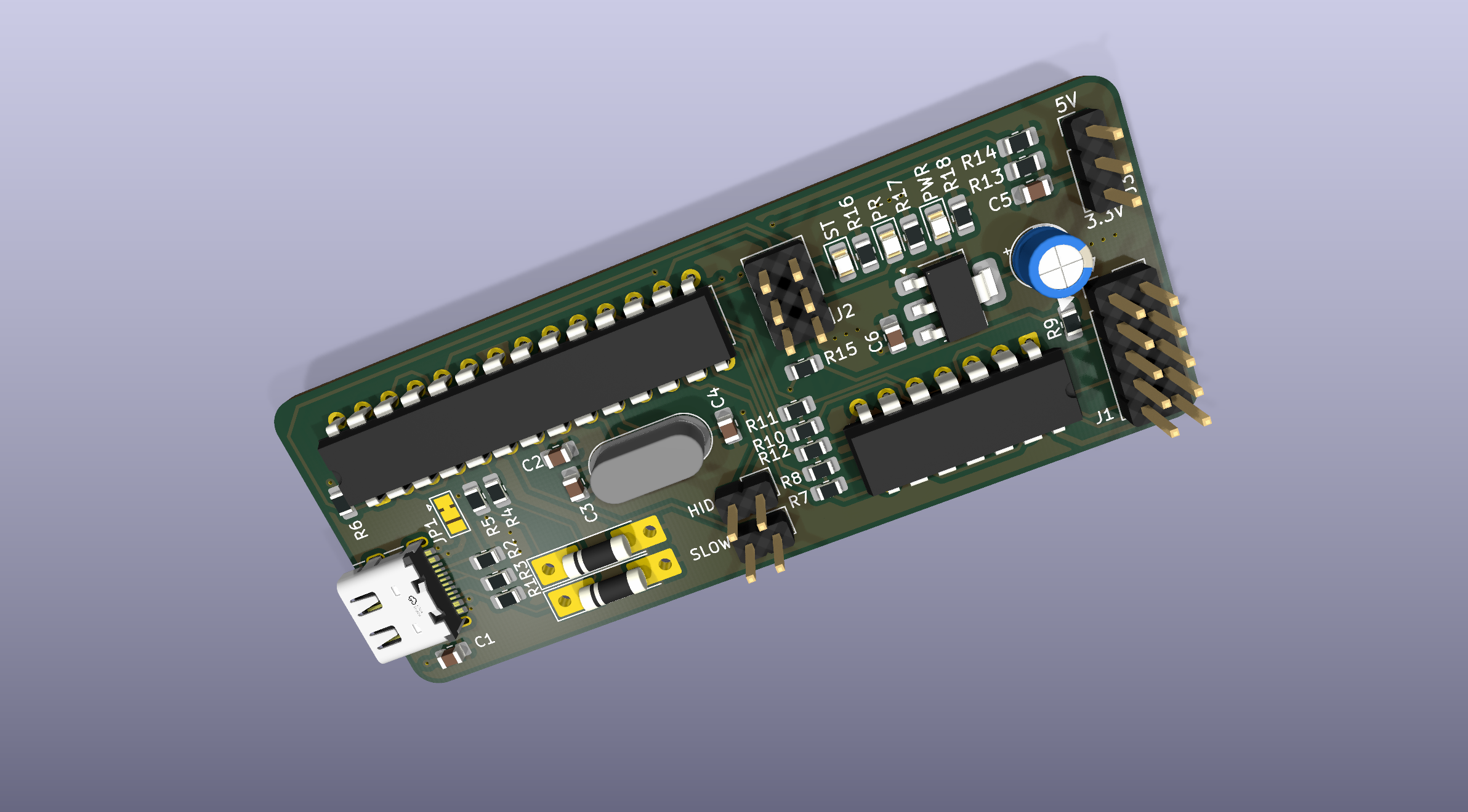
VCCINT, HID, and SLOW configuration headersST), and programming (PR) indicators| Connector | Purpose |
|---|---|
| USB-C | Connects AVR-Doper RE to the host computer |
| J1 | Connects AVR-Doper RE to the target AVR circuit |
| J2 | Programs the onboard ATmega328P controller |
J3 VCCINT | Selects 5 V, 3.3 V, or externally supplied target power |
J4 HID | Firmware mode input |
J5 SLOW | Slow programming-clock input |
The behavior of the HID and SLOW headers depends on the firmware loaded on the programmer.
J3 controls the voltage used by the target-facing ISP buffer and J1 pin 2 (VCCINT). Viewed from the component side, pin 1 is the end marked 5V and pin 3 is the end marked 3.3V.
| J3 setting | VCCINT source |
|---|---|
| Jumper on pins 1–2 | Onboard USB 5 V |
| Jumper on pins 2–3 | Onboard regulated 3.3 V |
| No jumper | Externally powered target through J1 pin 2 |
Install only one jumper. Never bridge all three pins or connect an onboard supply to a target that is already powered from another source.
J1 is an unkeyed 2×5 header. It is not the conventional Atmel 10-pin ISP connector.
Viewed from the component side of the PCB, with the square pin-1 pad at the upper left:
 1  TMOSI       2  VCCINT
 3  CLK         4  GND
 5  TRESET      6  GND
 7  TSCK        8  RX
9 TMISO 10 TX| Pin | Signal | Pin | Signal |
|---|---|---|---|
| 1 | TMOSI | 2 | VCCINT |
| 3 | CLK | 4 | GND |
| 5 | TRESET | 6 | GND |
| 7 | TSCK | 8 | RX |
| 9 | TMISO | 10 | TX |
Because J1 is not keyed, always identify pin 1 by its square PCB pad before attaching a cable. The pinout appears mirrored when viewed from the mating side of the cable connector.
J2 uses the standard 6-pin AVR ISP arrangement and is intended for loading firmware into the onboard ATmega328P.
| Pin | Signal | Pin | Signal |
|---|---|---|---|
| 1 | MISO | 2 | +5V |
| 3 | SCK | 4 | MOSI |
| 5 | RESET | 6 | GND |
Produced V4 boards have the USB pull-up selector (marked JP1) bridged on pads 1–2. Before first use, disconnect USB and target power, cut the copper link between pads 1–2, and solder-bridge pads 2–3 instead. Do not leave both sides bridged.
HID and SLOW as required by the loaded firmware and target circuit.Install a current AVRDUDE build with USB HID support, then configure AVR-Doper RE for HID mode. AVR-Doper uses the STK500v2 protocol; -P avrdoper tells AVRDUDE to use its AVR-Doper HID transport instead of a serial port.
Check communication and read the target's device signature:
avrdude -c stk500v2 -P avrdoper -p atmega328pWrite an Intel HEX file to target flash and verify it:
avrdude -c stk500v2 -P avrdoper -p atmega328p -U flash:w:firmware.hex:iRead target flash into an Intel HEX file:
avrdude -c stk500v2 -P avrdoper -p atmega328p -U flash:r:backup.hex:iReplace atmega328p with the connected target's AVRDUDE part name and replace the filenames as required. Run avrdude -p ? to list supported targets.
With the firmware included in this repository, AVRDUDE's connection summary reports the voltage present on VCCINT as Vtarget. Expect a reading close to 5.0 V with J3 on pins 1–2 or 3.3 V with J3 on pins 2–3. With J3 open, the reading reflects the voltage supplied by a self-powered target. Small differences are normal.
Vtarget is informational only. Select the correct J3 position before connecting the target; AVRDUDE cannot change the board's physical voltage selector.
AVR-Doper RE can power a 3.3 V target directly or work with a target that has its own 3.3 V supply.
The board must use a 74HC126, which can operate from 3.3 V. Do not substitute a 74HCT126, which requires a higher supply voltage.
J1 CLK, RX, and TX do not pass through the target-voltage buffer. Leave these auxiliary signals disconnected unless their voltage compatibility with the target has been verified.
Install PlatformIO Core, then run this command from the repository root:
pio run -d firmwareThe resulting image is firmware/.pio/build/uno/firmware.hex. Program it into the onboard ATmega328P through J2 using an external AVR ISP programmer. See the firmware notes for source layout, provenance, and licensing.
AVR-Doper RE is derived from the original AVR-Doper project by Objective Development. Credit for the original AVR-Doper concept, circuit, firmware, and V-USB-based implementation belongs to Christian Starkjohann, Objective Development, and the original contributors.
This respin is not affiliated with or endorsed by Objective Development.
| Qty | Value | Footprint | References |
|---|---|---|---|
| 6 | 10K | Resistor_SMD:R_0805_2012Metric_Pad1.20x1.40mm_HandSolder | R6, R7, R8, R10, R11, R12 |
| 3 | 270 | Resistor_SMD:R_0805_2012Metric_Pad1.20x1.40mm_HandSolder | R16, R17, R18 |
| 2 | 1K | Resistor_SMD:R_0805_2012Metric_Pad1.20x1.40mm_HandSolder | R9, R15 |
| 2 | 22pF | Capacitor_SMD:C_0805_2012Metric_Pad1.18x1.45mm_HandSolder | C3, C4 |
| 2 | 3V6 | Diode_SMD:D_MELF-RM10_Universal_Handsoldering | D1, D2 |
| 2 | 4u7 | Capacitor_SMD:C_0805_2012Metric_Pad1.18x1.45mm_HandSolder | C1, C5 |
| 2 | 5.1K 1% | Resistor_SMD:R_0805_2012Metric_Pad1.20x1.40mm_HandSolder | R1, R2 |
| 2 | 68 | Resistor_SMD:R_0805_2012Metric_Pad1.20x1.40mm_HandSolder | R4, R5 |
| 1 | 100nF | Capacitor_SMD:C_0805_2012Metric_Pad1.18x1.45mm_HandSolder | C2 |
| 1 | 10uF | Capacitor_SMD:C_0805_2012Metric_Pad1.18x1.45mm_HandSolder | C6 |
| 1 | 16M | Crystal:Crystal_HC49-4H_Vertical | Y1 |
| 1 | 22K | Resistor_SMD:R_0805_2012Metric_Pad1.20x1.40mm_HandSolder | R14 |
| 1 | 2K2 | Resistor_SMD:R_0805_2012Metric_Pad1.20x1.40mm_HandSolder | R3 |
| 1 | 33K | Resistor_SMD:R_0805_2012Metric_Pad1.20x1.40mm_HandSolder | R13 |
| 1 | 47uF | Capacitor_THT:CP_Radial_D5.0mm_P2.00mm | C7 |
| 1 | 74HC126 | Package_DIP:DIP-14_W7.62mm | U2 |
| 1 | AMS1117-3.3 | Package_TO_SOT_SMD:SOT-223-3_TabPin2 | U3 |
| 1 | ATmega328-P | Package_DIP:DIP-28_W7.62mm | U1 |
| 1 | GT-USB-7010ASV | Connector_USB:USB_C_Receptacle_G-Switch_GT-USB-7010ASV | USB_C_Receptacle1 |
| 1 | HID | Connector_PinHeader_2.54mm:PinHeader_1x02_P2.54mm_Vertical | J4 |
| 1 | LOGO | Xinj_Footprints:logo_2020 | G*** |
| 1 | PINHD_2x3_Male | Connector_PinHeader_2.54mm:PinHeader_2x03_P2.54mm_Vertical | J2 |
| 1 | PINHD_2x5_Male | Connector_PinHeader_2.54mm:PinHeader_2x05_P2.54mm_Vertical | J1 |
| 1 | PR | LED_SMD:LED_0805_2012Metric_Pad1.15x1.40mm_HandSolder | D4 |
| 1 | PWR | LED_SMD:LED_0805_2012Metric_Pad1.15x1.40mm_HandSolder | D5 |
| 1 | SLOW | Connector_PinHeader_2.54mm:PinHeader_1x02_P2.54mm_Vertical | J5 |
| 1 | ST | LED_SMD:LED_0805_2012Metric_Pad1.15x1.40mm_HandSolder | D3 |
| 1 | SolderJumper_3_Bridged12 | Jumper:SolderJumper-3_P1.3mm_Bridged12_Pad1.0x1.5mm | JP1 |
| 1 | VCCINT | Connector_PinHeader_2.54mm:PinHeader_1x03_P2.54mm_Vertical | J3 |
fossasia/pslab-hardware
PSLab Hardware Design and Schematics https://pslab.io


dshills/KiCadAI
AI-assisted KiCad design toolkit with Go CLI, direct schematic/PCB writers, validation, and pinmap checks.

JMET04/aicad-agent
Deterministic CAD/EDA agent plugin for 2D drawings, AutoCAD, SolidWorks, KiCad, review gates and auditable delivery.
It measures 75 × 30 mm and has 2 copper layers, 1.6 mm thick.
42 parts, built around the ATMEGA328-PU, 74HC126D, AMS1117-3.3 and GRM21BR61A106KE19L. The full list of its parts is on this page, with links to each part's symbol and footprint where PCBKit's library has them.
From the alexjx/avrdoper-re repository on GitHub, at the commit this page was made from: the board is hardware/avrdoper_re.kicad_pcb and its schematic hardware/avrdoper_re.kicad_sch. PCBKit opens the board in the browser, with nothing to install.
Its repository states no licence, so its author keeps all rights: ask alexjx before reusing the design.