
4 layers108 × 69 mm
Fmc2sata
antmicro/fmc-sata-adapter
Adapter board exposing SATA M.2 SSD on FMC board-to-board connector
65 parts17Apache-2.0

 akashh218/Variable-DC-DC-Buck-Converter
A custom 5A variable buck converter designed in KiCad, supporting a 4–17V input range and an adjustable 1–7V output, with a focus on compact power-stage layout, efficient power delivery, thermal management, and practical DC-DC power conversion.
Buck converter is an open-source printed circuit board by akashh218, from the akashh218/Variable-DC-DC-Buck-Converter repository on GitHub. It is a 2-layer board of 34.7 × 11.3 mm with 15 parts on 7 nets, routed with 56 tracks and 2 vias.
It is built around the TPS565208DDC. Its parts include 8 capacitors, 2 resistors, 1 IC and 1 inductor. It belongs with the power boards of this library.
A custom 5A variable buck converter designed in KiCad, supporting a 4–17V input range and an adjustable 1–7V output. The design focuses on efficient DC-DC power conversion, compact power-stage layout, proper grounding, decoupling, thermal considerations, and practical power electronics design.
This project involves the complete design of a variable-output buck converter, from schematic design and component selection through PCB placement, routing, and 3D visualization.
The converter is designed around the TPS56208 synchronous buck converter, with a potentiometer-based feedback network for adjustable output voltage.
The target design provides a compact and practical power supply suitable for powering embedded systems, sensors, motors, controllers, and other low-voltage electronics.
The main power-conversion stage is built around the TPS56208 buck converter.
The input voltage is filtered using multiple capacitors before entering the converter. The switching node drives the 3.3µH inductor, which forms the main energy-storage element of the buck converter.
The output is filtered using multiple capacitors to reduce switching ripple and provide a stable DC output.
The feedback network uses fixed resistors together with a 250kΩ potentiometer, allowing the output voltage to be adjusted over the intended range.
| Parameter | Specification |
|---|---|
| Input Voltage | 4–17V DC |
| Output Voltage | 1–7V adjustable |
| Maximum Output Current | 5A target |
| Switching Regulator | TPS56208 |
| Inductor | 3.3µH |
| Feedback Adjustment | 250kΩ potentiometer |
| Input Connector | 2-pin terminal |
| Output Connector | 2-pin terminal |
| PCB Design Tool | KiCad |
Note: The 5A figure is a design target. Actual continuous output current depends on the TPS56208's thermal limits, PCB copper area, inductor rating, switching conditions, and cooling. It should be validated through hardware testing rather than assumed from the schematic alone.
The PCB was designed with particular attention to:
The power components were placed close to the regulator to minimize parasitic resistance and inductance in the high-current switching paths.
The main power path consists of:
VIN → TPS56208 → SW → 3.3µH Inductor → VOUT
The input capacitors provide local energy storage for the switching regulator, while the output capacitors smooth the inductor current and reduce output voltage ripple.
The feedback network continuously monitors the output voltage and adjusts the regulator's duty cycle to maintain the selected output voltage.
The output voltage is controlled through the feedback divider.
The fixed resistors establish the feedback network, while the 250kΩ potentiometer provides variable adjustment.
Rotating the potentiometer changes the feedback voltage seen by the regulator, allowing the output to be adjusted within the designed voltage range.
The PCB uses a compact two-layer power-oriented layout with emphasis on minimizing high-current paths.
Important layout considerations include:
Some of the main challenges during development included:
This repository contains the design files associated with the project, including:
PCB Design Completed
The next stage is hardware fabrication and electrical validation.
Testing should include:
This project strengthened my practical understanding of:
Designed in KiCad | TPS56208 | 4–17V Input | 1–7V Adjustable Output | 5A Target
| Qty | Value | Footprint | References |
|---|---|---|---|
| 2 | 0.1uF | Capacitor_SMD:C_0603_1608Metric | C4, C5 |
| 2 | 10uF | Capacitor_SMD:C_0603_1608Metric | C3, C8 |
| 2 | 22uF | Capacitor_SMD:C_0805_2012Metric | C6, C7 |
| 2 | 33uF | Capacitor_SMD:C_0805_2012Metric | C1, C2 |
| 1 | 10k | Resistor_SMD:R_0402_1005Metric | R2 |
| 1 | 250K | r potentiometer:TRIM_3296W-1-201LF | RV1 |
| 1 | 3.3uH | inductor:IND_VLCF5020T-3R3N2R0-1 | L1 |
| 1 | 82k | Resistor_SMD:R_0402_1005Metric | R1 |
| 1 | I/P | Connector_JST:JST_EH_B2B-EH-A_1x02_P2.50mm_Vertical | VIN |
| 1 | O/P | Connector_JST:JST_EH_B2B-EH-A_1x02_P2.50mm_Vertical | VOUT |
| 1 | TPS565208 | Package_TO_SOT_SMD:SOT-23-6 | U1 |
antmicro/fmc-sata-adapter
Adapter board exposing SATA M.2 SSD on FMC board-to-board connector

RICCIARDI-Adrien/Cyclope
Raspberry Pi powered robot with camera live stream and 360° lidar.

Fiberprinter/fiberprinter-electronics
Fiberelectronics Control every pulse, master every micron

InSynchronous/mango
An ESP32-S3 based flight computer with an external flash, imu, barometer, magnetometer, 4 servo ports, and 4 pyrotechnic channels with MOSFETs. Designed for Aerospace applications.
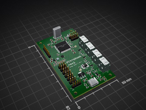
InSynchronous/UltraHawk
A custom flight computer designed for drones and flight computers.

ben-labs-ltd/BL-N305X
Meshtastic intended LoRa Node - Ben Labs Node 30.5dBm

Gold-Rush-Robotics/pcb_2024
A repository to store work done on PCBs for the 2024 season

akashh218/Voice-and-AI-Enabled-Intelligent-Robot-Controller-PCB
Custom 4-layer PCB for a voice and AI-enabled intelligent robot, integrating ESP32 control, dual DC motors, three servos, voice recognition, AI audio interaction, temperature monitoring, RGB LEDs, and expansion…
It measures 34.7 × 11.3 mm and has 2 copper layers, 1.6 mm thick.
15 parts, built around the TPS565208DDC. The full list of its parts is on this page, with links to each part's symbol and footprint where PCBKit's library has them.
From the akashh218/Variable-DC-DC-Buck-Converter repository on GitHub, at the commit this page was made from: the board is buck converter/buck converter.kicad_pcb and its schematic buck converter/buck converter.kicad_sch. PCBKit opens the board in the browser, with nothing to install.
Its repository states no licence, so its author keeps all rights: ask akashh218 before reusing the design.