


2 layers42.5 × 28.8 mm
C5VRX JACK DIY V3
Twotoz/C5VRX
Ultra-minimal, zero-CPU 5.8 GHz analog FPV video receiver using ESP32-C5 Wi-Fi 6 PHY MODEM_DIAG, BitScrambler WBFM demodulation & resistor DAC CVBS
18 parts515GPL-3.0

 Twotoz/C5VRX515
Ultra-minimal, zero-CPU 5.8 GHz analog FPV video receiver using ESP32-C5 Wi-Fi 6 PHY MODEM_DIAG, BitScrambler WBFM demodulation & resistor DAC CVBS
C5VRX JACK DIY V2 is an open-source printed circuit board by Twotoz, from the Twotoz/C5VRX repository on GitHub, published under the GPL-3.0 licence. It is a 2-layer board of 42.5 × 28.8 mm with 18 parts on 25 nets, routed with 53 tracks and 2 vias.
It is built around the PJ-320D. Its parts include 9 resistors, 2 connectors, 1 capacitor and 1 IC. It belongs with the radio and wireless and audio and music boards and the ESP32 and RISC-V boards of this library.
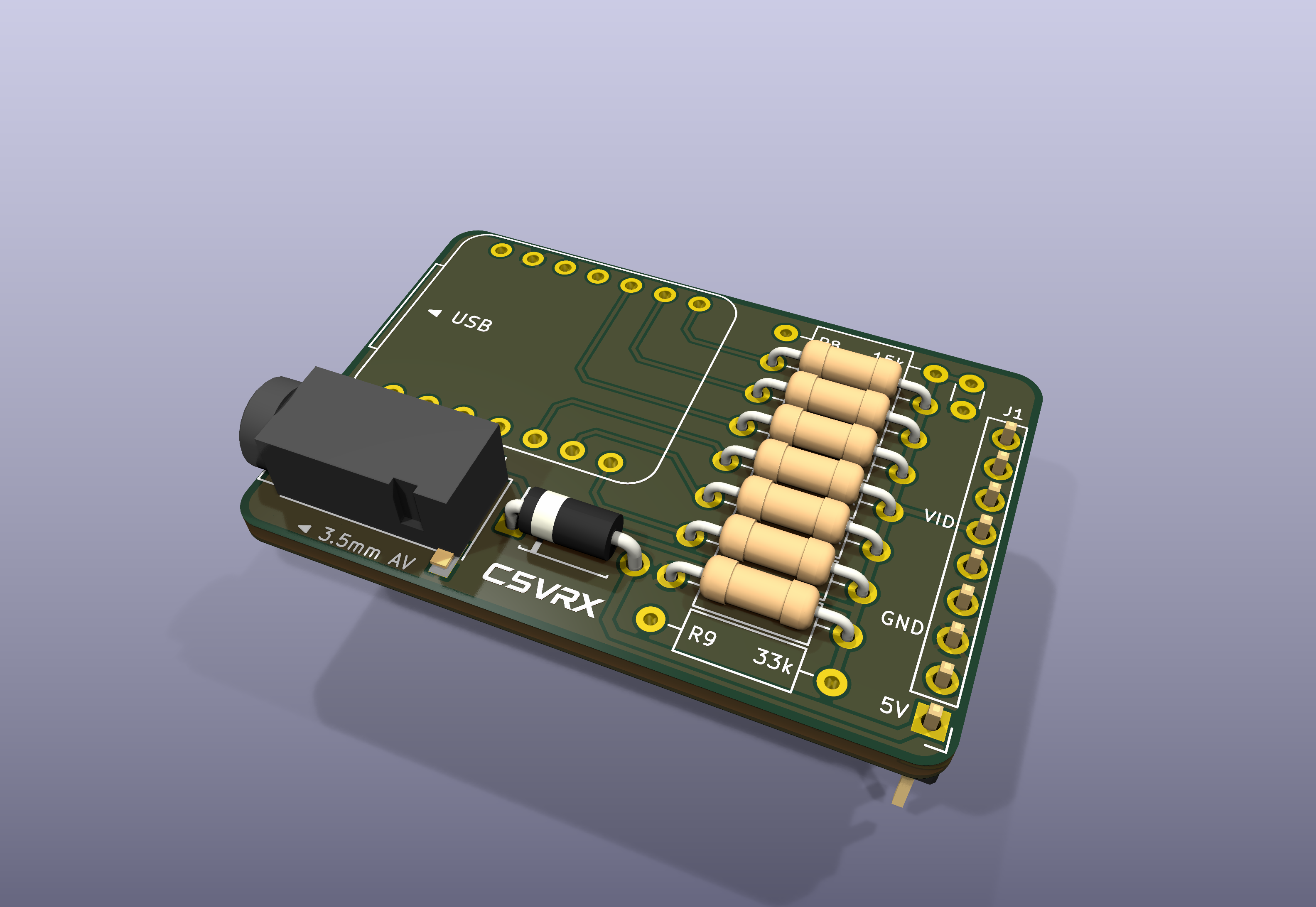
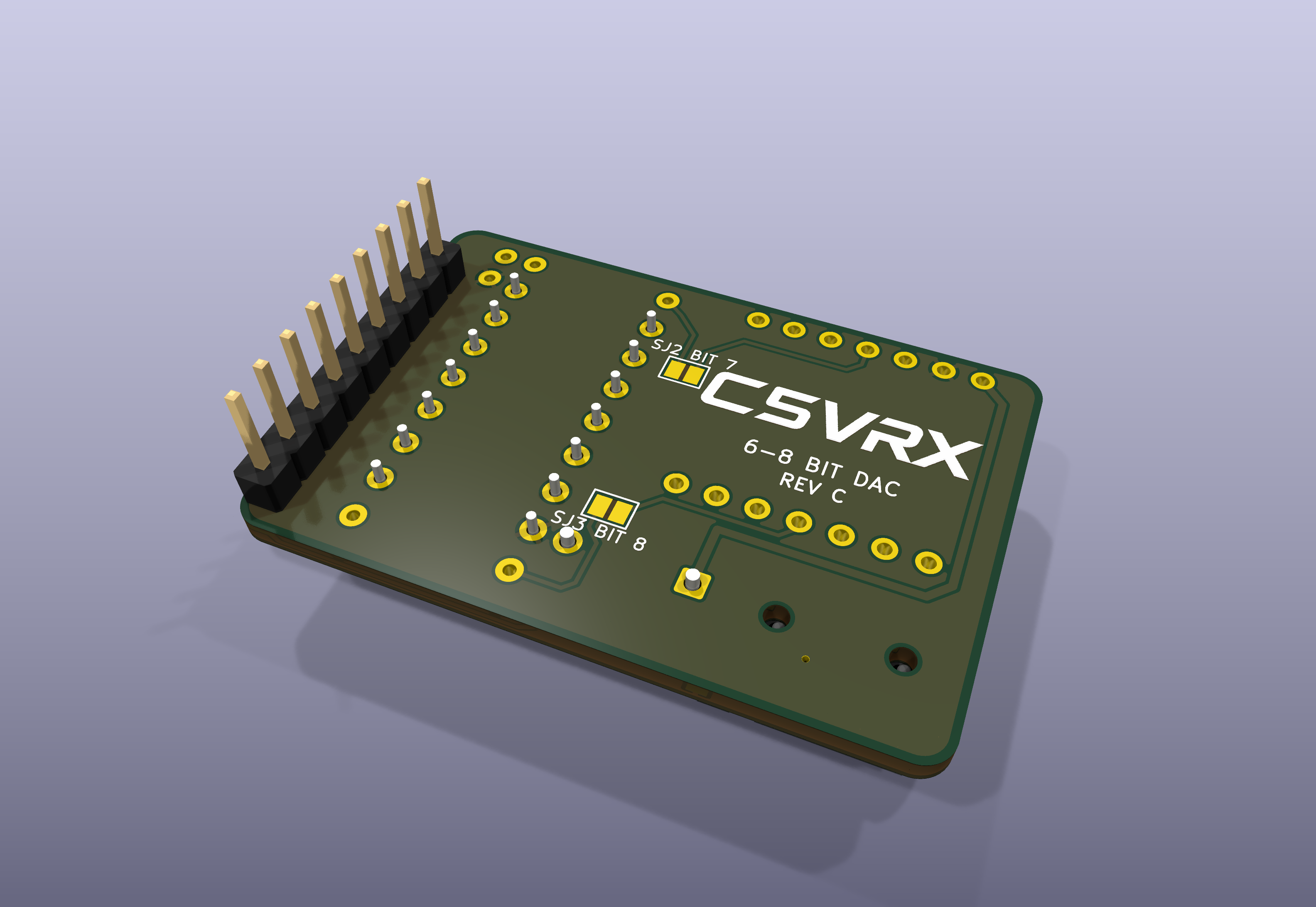
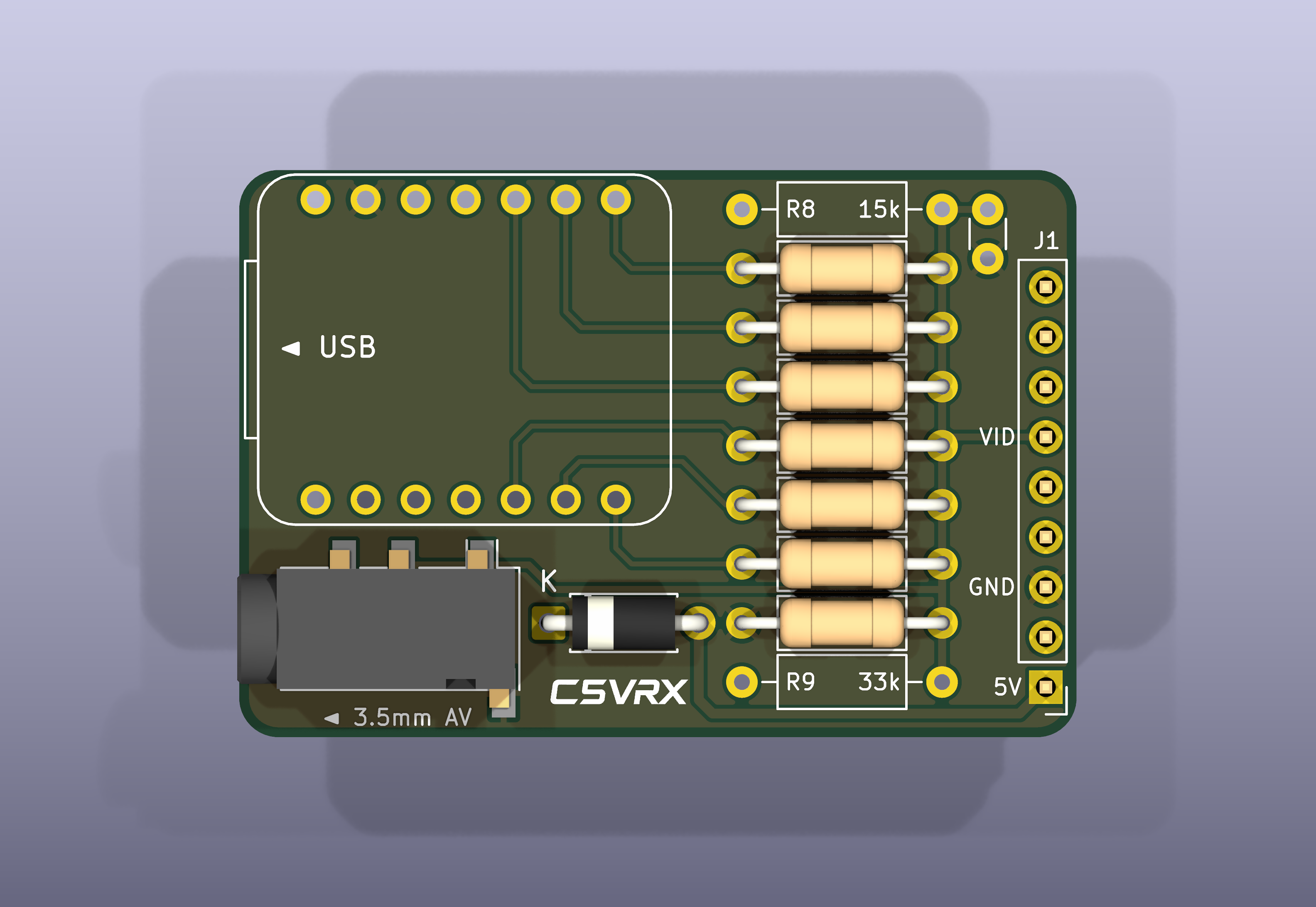
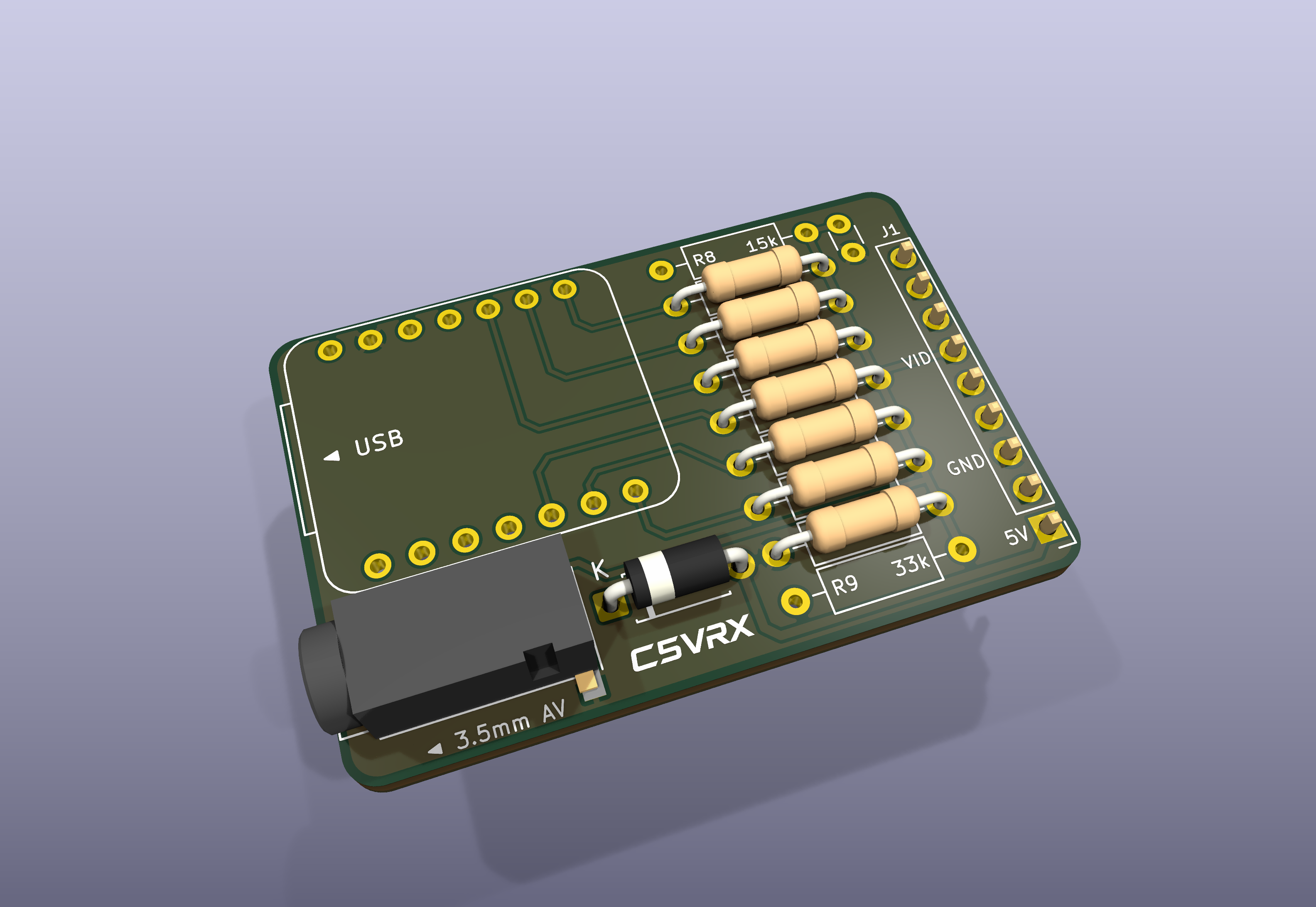
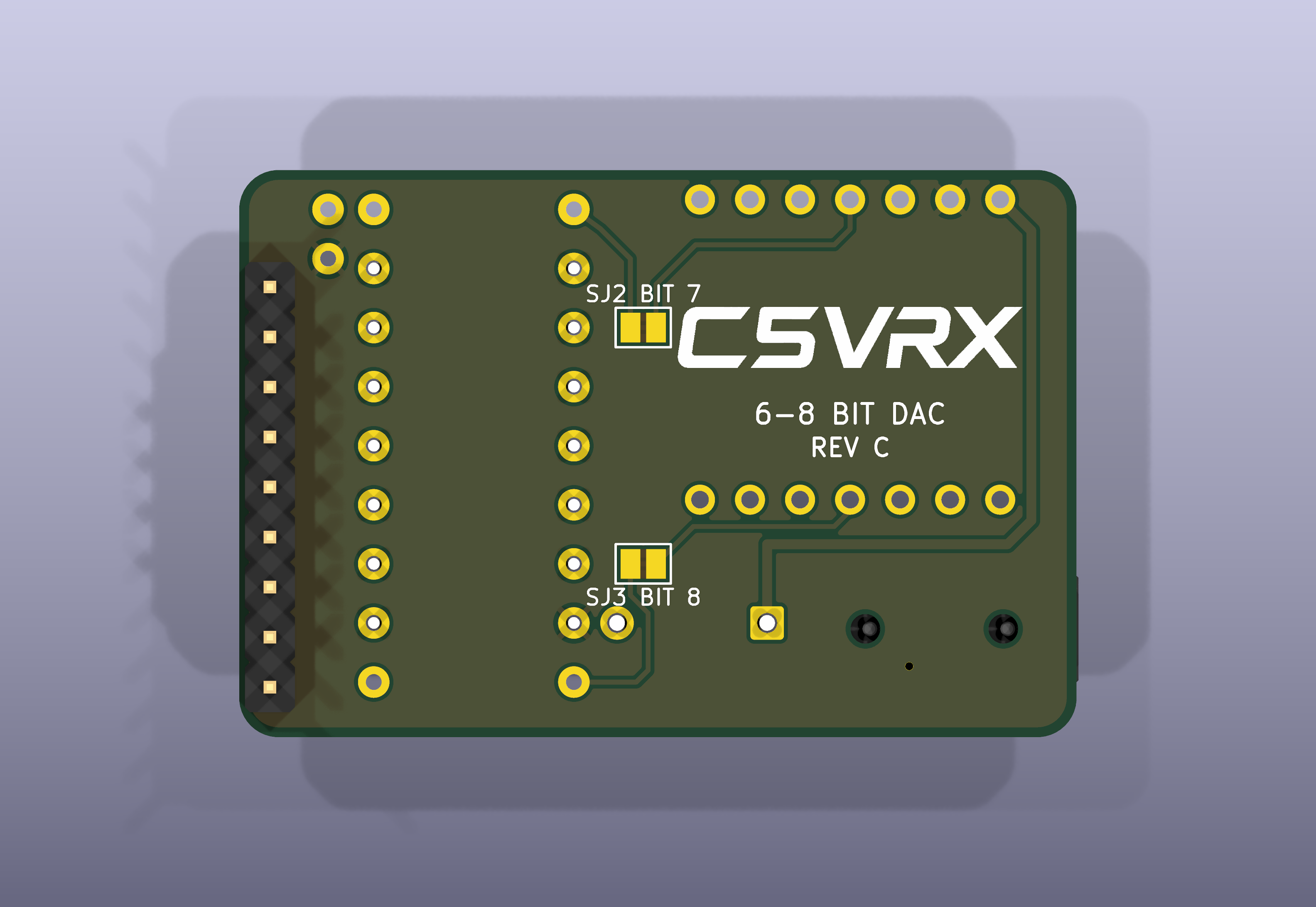
A two-layer DIY carrier for the Seeed Studio XIAO ESP32-C5, with a Fat Shark module-bay header and PJ-320D 3.5 mm AV jack. REV C keeps the REV B outline (42.51 × 28.80 mm), part positions and DAC branches, and replaces the SJ1 bay-power solder bridge with a through-hole Schottky diode.
| File | Link |
|---|---|
| Gerber X2 + Excellon drills | Fabrication ZIP |
| KiCad 10 source | Project · PCB · Schematic |
| Parts and assembly flags | BOM |
| Schematic and fit check | Schematic PDF · 1:1 PDF |
| Mechanical models | STEP · GLB |
| High-resolution images | Front · Back · Low angle · All five as ZIP |
C5VRX:D_DO-41_P7.62mm_Horizontal_Compact): 7.62 mm lead pitch, 1.7 mm pads and 1.0 mm drills, so its courtyard fits between the jack and the resistor bank.The XIAO's 5 V rail is about 0.3 V lower on bay power (diode drop); the XIAO regulates its own 3.3 V from it. With USB and the bay connected at the same time, the higher of the two supplies feeds the XIAO.
| Jumper | Function | Default |
|---|---|---|
| SJ2 / BIT 7 | Connect D10 / GPIO10 through R8 (15 kΩ) to VIDEO | Open |
| SJ3 / BIT 8 | Connect D3 / GPIO7 through R9 (33 kΩ) to VIDEO | Open |
R8 is 15 kΩ and R9 is 33 kΩ; R1–R7 and the 200 Ω load are unchanged. R8 and R9 are DNP with the current six-bit firmware. The jumpers only connect hardware branches; they do not select a firmware mode. These are new low bits: in a future seven-bit implementation D10 is bit 0; in an eight-bit implementation D10 is bit 1, D3 is bit 0, and the existing D4–D9 outputs are bits 2–7.
| Output configuration | SJ2 | SJ3 | Additional resistors |
|---|---|---|---|
| Current six-bit | Open | Open | R8/R9 DNP |
| Future seven-bit | Closed | Open | Fit R8 |
| Future eight-bit | Closed | Closed | Fit R8 and R9 |
Wider output requires matching firmware and loaded CVBS level/linearity measurements; it is not enabled or hardware-qualified by this PCB. D3/GPIO7 is a boot-strapping pin: validate repeated cold boots and reset loading before fitting/enabling R9. Keep the extra resistors unpopulated and jumpers open with current firmware.
R1–R7 retain the existing 8.2 kΩ / 3.9 kΩ / 2 kΩ / 1 kΩ / 470 Ω / 240 Ω branches and 200 Ω shunt. All resistors use DIN0207 axial through-hole footprints, 10.16 mm lead pitch; 1% is recommended. C1 is optional 470 pF / DNP. No additional 75 Ω shunt is fitted. J2 tip and ring 1 carry VIDEO, sleeve is GND, and ring 2 is unconnected.
C5VRX_JACK_DIY_V3.kicad_pro in KiCad 10. Project symbol/footprint libraries (including the D1 footprint) and the PJ-320D STEP model are included.exports/.Digital checks are not physical qualification. REV C has not yet been built or measured. REV B and REV A remain available.
This carrier adapts the existing hardware/C5VRX_JACK_DIY and hardware/C5VRX_JACK_DIY_V2 (REV B) boards and DAC design from C5VRX by Twotoz and the C5VRX contributors. REV C replaces the SJ1 power jumper with the D1 Schottky diode and reroutes the affected 5 V and BIT 8 traces; the D1 footprint is derived from KiCad's Diode_THT:D_DO-41_SOD81_P7.62mm_Horizontal with smaller pads.
Canonical source: Twotoz/C5VRX. Visit the official C5VRX website for the project and its Discord invite. Applicable source terms are in LICENSE; separate name/logo terms remain in BRANDING.md. This proposed hardware revision is not a claim of an already released or physically validated product.
| Qty | Value | Footprint | References |
|---|---|---|---|
| 1 | 15k | Resistor_THT:R_Axial_DIN0207_L6.3mm_D2.5mm_P10.16mm_Horizontal | R8 |
| 1 | 1k | Resistor_THT:R_Axial_DIN0207_L6.3mm_D2.5mm_P10.16mm_Horizontal | R4 |
| 1 | 200 | Resistor_THT:R_Axial_DIN0207_L6.3mm_D2.5mm_P10.16mm_Horizontal | R7 |
| 1 | 240 | Resistor_THT:R_Axial_DIN0207_L6.3mm_D2.5mm_P10.16mm_Horizontal | R6 |
| 1 | 2k | Resistor_THT:R_Axial_DIN0207_L6.3mm_D2.5mm_P10.16mm_Horizontal | R3 |
| 1 | 3.9k | Resistor_THT:R_Axial_DIN0207_L6.3mm_D2.5mm_P10.16mm_Horizontal | R2 |
| 1 | 33k | Resistor_THT:R_Axial_DIN0207_L6.3mm_D2.5mm_P10.16mm_Horizontal | R9 |
| 1 | 470 | Resistor_THT:R_Axial_DIN0207_L6.3mm_D2.5mm_P10.16mm_Horizontal | R5 |
| 1 | 470pF | Capacitor_THT:C_Disc_D3.0mm_W1.6mm_P2.50mm | C1 |
| 1 | 5V LINK | Jumper:SolderJumper-2_P1.3mm_Open_Pad1.0x1.5mm | SJ1 |
| 1 | 8.2k | Resistor_THT:R_Axial_DIN0207_L6.3mm_D2.5mm_P10.16mm_Horizontal | R1 |
| 1 | BIT 7 | Jumper:SolderJumper-2_P1.3mm_Open_Pad1.0x1.5mm | SJ2 |
| 1 | BIT 8 | Jumper:SolderJumper-2_P1.3mm_Open_Pad1.0x1.5mm | SJ3 |
| 1 | C5VRX Front Logo | C5VRX:C5VRX_Logo_Front_Small | LOGO2 |
| 1 | C5VRX logo | C5VRX:C5VRX_Logo_Back | LOGO1 |
| 1 | FATSHARK BAY | C5VRX:FatShark_Header_1x09 | J1 |
| 1 | PJ-320D | Connector_Audio:Jack_3.5mm_PJ320D_Horizontal | J2 |
| 1 | XIAO ESP32-C5 | C5VRX:XIAO-ESP32-C5-DIP | U1 |
Twotoz/C5VRX
Ultra-minimal, zero-CPU 5.8 GHz analog FPV video receiver using ESP32-C5 Wi-Fi 6 PHY MODEM_DIAG, BitScrambler WBFM demodulation & resistor DAC CVBS

Twotoz/C5VRX
Ultra-minimal, zero-CPU 5.8 GHz analog FPV video receiver using ESP32-C5 Wi-Fi 6 PHY MODEM_DIAG, BitScrambler WBFM demodulation & resistor DAC CVBS

GeekFunkLabs/squishbox
Software and design files for a Raspberry Pi sound module enclosure


SharKingStudios/Fracture
An infinitely expandable, velocity sensing split midi keyboard.


rh1tech/frank-lab
FRANK Board Laboratory (work-in-progress board prototopyes)


It measures 42.5 × 28.8 mm and has 2 copper layers, 1.6 mm thick.
18 parts, built around the PJ-320D. The full list of its parts is on this page, with links to each part's symbol and footprint where PCBKit's library has them.
From the Twotoz/C5VRX repository on GitHub, at the commit this page was made from: the board is hardware/C5VRX_JACK_DIY_V2/C5VRX_JACK_DIY_V2.kicad_pcb and its schematic hardware/C5VRX_JACK_DIY/C5VRX_JACK_DIY.kicad_sch. PCBKit opens the board in the browser, with nothing to install.
Its repository publishes it under the GPL-3.0 licence: you may reuse it on that licence's terms (keep the author's notice, and for a copyleft licence share your changes alike).