
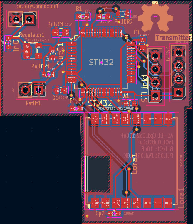
2 layers152.1 × 70.1 mm

A real-time wireless tracking system using an STM32-based transmitter integrated with GPS and LoRa modules, and an ESP32-based receiver with LoRa communication. This project demonstrates wireless long range communication using RF signals.
PCB Design is an open-source printed circuit board by Pritika-2024, from the Pritika-2024/Lora_Communication_based_real_time_tracking repository on GitHub, published under the MIT licence. It is a 2-layer board of 36.5 × 42.5 mm with 20 parts on 62 nets, routed with 158 tracks and 21 vias.
It is built around the NEO-6M, SX1278 and AP2112K-3.3. It belongs with the radio and wireless boards and the STM32 boards of this library.


This project implements a long-range wireless tracking system using LoRa communication. An STM32-based transmitter acquires real-time GPS coordinates and transmits them over LoRa, while an ESP32-based receiver processes and displays the received data. The system is optimized for low-power, long-distance IoT tracking.
The system consists of two nodes:
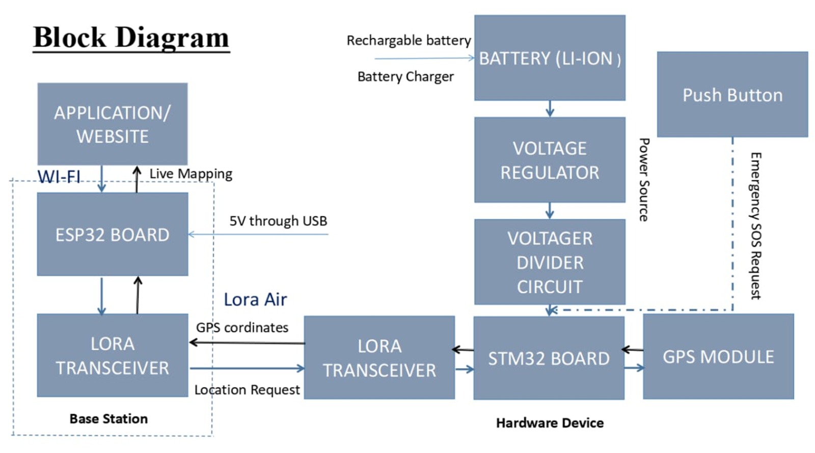
LoRa (SX1278 → STM32)
GPS (NEO-6M → STM32)
ST-Link (Programming)
The transmitter circuit integrates STM32 with GPS (UART) and LoRa (SPI). A custom PCB was designed in KiCad for compact integration.
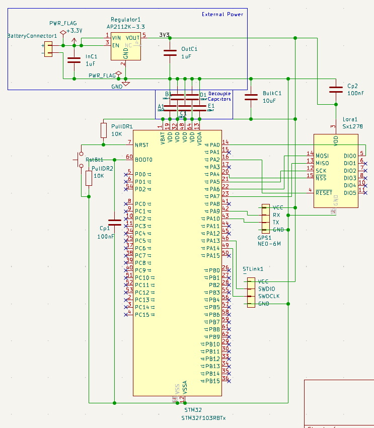
The system is powered using an external battery connected via a 2-pin header (BatteryConnector1).
Battery → Regulator (3.3V) →
STM32, LoRa, GPS
Ensures stable 3.3V operation for all modules.
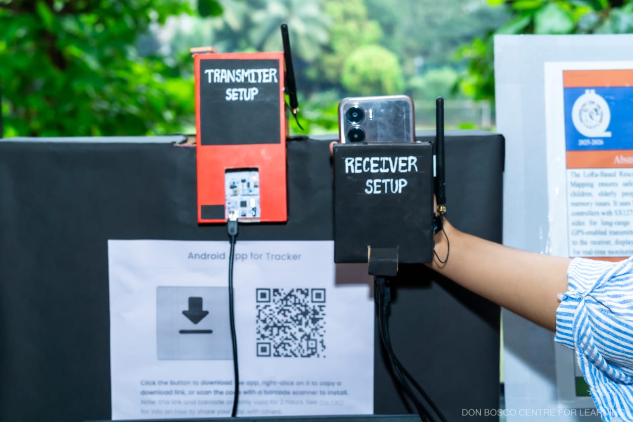
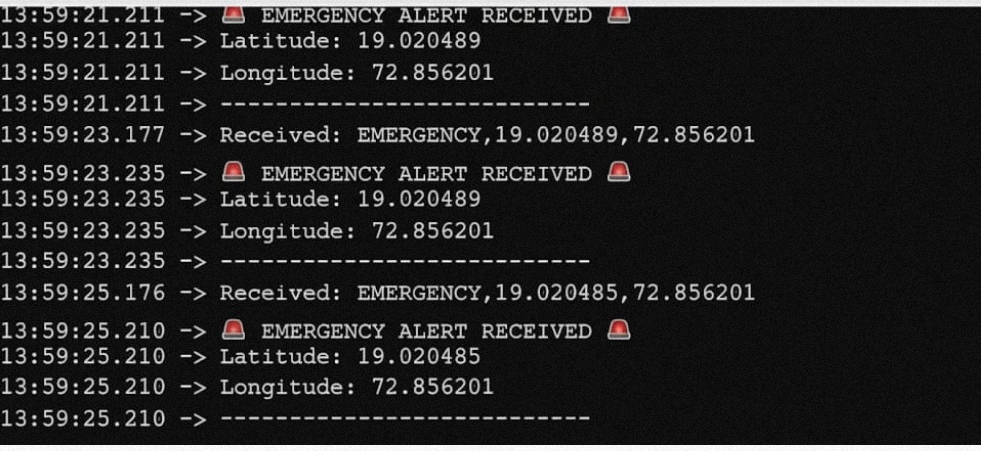
The hardware prototype validates real-time communication between transmitter and receiver.
| File | Description |
|---|---|
src/transmitter.cpp | STM32 code for GPS data acquisition and LoRa transmission |
src/receiver.cpp | ESP32 code for LoRa reception and data decoding |
LoRa.h
Used for interfacing with SX1278 module using SPI and handling packet transmission/reception.
TinyGPS++
Parses raw NMEA data from GPS module into usable latitude and longitude values.
SPI.h
Enables SPI communication between STM32/ESP32 and LoRa module.
SoftwareSerial (if used)
Provides UART interface when hardware UART is limited (mainly for GPS).
| Qty | Value | Footprint | References |
|---|---|---|---|
| 7 | 100nF | Capacitor_SMD:C_0603_1608Metric | A1, B1, C1, Cp1, Cp2, D1, E1 |
| 2 | 10K | Resistor_SMD:R_0603_1608Metric | PullDR1, PullDR2 |
| 2 | 1uF | Capacitor_SMD:C_0603_1608Metric | InC1, OutC1 |
| 2 | ~ | Connector_PinHeader_2.54mm:PinHeader_1x02_P2.54mm_Vertical | BatteryConnector1, RstBt1 |
| 1 | - | Connector_PinHeader_2.54mm:PinHeader_1x04_P2.54mm_Vertical | STLink1 |
| 1 | 10uF | Capacitor_SMD:C_0805_2012Metric | BulkC1 |
| 1 | AP2112K-3.3 | Package_TO_SOT_SMD:SOT-23-5 | Regulator1 |
| 1 | NEO-6M | Connector_PinHeader_2.54mm:PinHeader_1x04_P2.54mm_Vertical | GPS1 |
| 1 | STM32F103RBTx | Package_QFP:LQFP-64_10x10mm_P0.5mm | STM32 |
| 1 | Sx1278 | RF_Module:Ai-Thinker-Ra-01-LoRa | Lora1 |
The 19 most common of 20 parts.


Arshsingh1602/Smart-Irrigation-System
This is our project of SIH 2024 in which we developed a smart irrigation system that can be used to control the under and overuse of water in the feild of farmer.

TanujRai14/Sat_pcb_design
This repository contains the PCB design files and documentation for a Can Satellite, featuring multiple environmental and orientation sensors, power management, and wireless communication capabilities.

Kmshanley/PicoSat-Initiative
The pocket cube standard requires satellites to be 5x5x5cm and under 250 grams. Upon completion of this Wentworth PicoSat it will become one of the smallest satellites capable of high resolution imagery from LEO.


GiZano/QuakeGuard
Distributed Earthquake Early Warning (EEW) system built on low-cost ESP32-C3 IoT sensors with Zero-Trust security, multi-node epicenter triangulation, and on-premise AI emergency reports.
It measures 36.5 × 42.5 mm and has 2 copper layers, 1.6 mm thick.
20 parts, built around the NEO-6M, SX1278 and AP2112K-3.3. The full list of its parts is on this page, with links to each part's symbol and footprint where PCBKit's library has them.
From the Pritika-2024/Lora_Communication_based_real_time_tracking repository on GitHub, at the commit this page was made from: the board is 02_PCB_Transmitter/PCB_Design.kicad_pcb and its schematic 02_PCB_Transmitter/Schematic.kicad_sch. PCBKit opens the board in the browser, with nothing to install.
Its repository publishes it under the MIT licence: you may reuse it on that licence's terms (keep the author's notice, and for a copyleft licence share your changes alike).