2 layers100 × 100 mm
 MyCloudExample/Kicad_Proyectos1
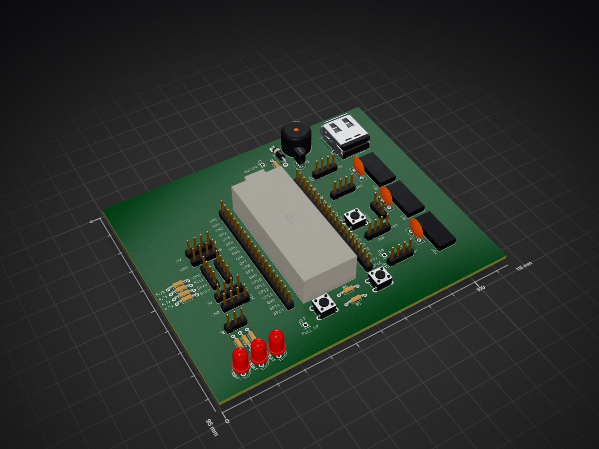
Placa de Desarrollo is an open-source printed circuit board by MyCloudExample, from the MyCloudExample/Kicad_Proyectos repository on GitHub. It is a 2-layer board of 115 × 95 mm with 44 parts on 51 nets, routed with 229 tracks and 0 vias.
It is built around the RP2350A and BC547. Its parts include 18 connectors, 10 resistors, 4 diodes, 3 capacitors and 3 switches. It belongs with the RP2350 boards of this library.


| Qty | Value | Footprint | References |
|---|---|---|---|
| 10 | Conn_01x04 | Connector_PinHeader_2.54mm:PinHeader_1x04_P2.54mm_Vertical | J5, J6, J7, J9, J10, J12, J13, J14, J15, J16 |
| 4 | 4,7k | Resistor_THT:R_Axial_DIN0204_L3.6mm_D1.6mm_P7.62mm_Horizontal | R1, R2, R3, R4 |
| 3 | 100nF | Capacitor_THT:C_Disc_D8.0mm_W2.5mm_P5.00mm | C1, C2, C3 |
| 3 | 10k | Potentiometer_THT:Potentiometer_Piher_T-16H_Single_Horizontal | RV2, RV3, RV4 |
| 3 | 220 | Resistor_THT:R_Axial_DIN0204_L3.6mm_D1.6mm_P7.62mm_Horizontal | R8, R9, R10 |
| 3 | Conn_01x01 | Connector_PinHeader_2.54mm:PinHeader_1x01_P2.54mm_Vertical | J4, J17, J18 |
| 3 | LED | LED_THT:LED_D5.0mm | D2, D3, D4 |
| 2 | 10K | Resistor_THT:R_Axial_DIN0204_L3.6mm_D1.6mm_P7.62mm_Horizontal | R5, R6 |
| 2 | Conn_01x03 | Connector_PinHeader_2.54mm:PinHeader_1x03_P2.54mm_Vertical | J8, J11 |
| 1 | 1K | Resistor_THT:R_Axial_DIN0204_L3.6mm_D1.6mm_P7.62mm_Horizontal | R7 |
| 1 | 1N4007 | Diode_THT:D_DO-41_SOD81_P10.16mm_Horizontal | D1 |
| 1 | BC547 | Package_TO_SOT_THT:TO-92_Inline | Q1 |
| 1 | Buzzer | Buzzer_Beeper:Buzzer_12x9.5RM7.6 | BZ1 |
| 1 | LEFT | Connector_PinHeader_2.54mm:PinHeader_1x20_P2.54mm_Vertical | J2 |
| 1 | PULL DOWN | Button_Switch_THT:SW_PUSH_6mm | SW2 |
| 1 | PULL UP | Button_Switch_THT:SW_PUSH_6mm | SW3 |
| 1 | RESET | Button_Switch_THT:SW_PUSH_6mm | SW1 |
| 1 | RIGHT | Connector_PinHeader_2.54mm:PinHeader_1x20_P2.54mm_Vertical | J3 |
| 1 | RP2350 | BoardF_Pi_Pico:BoardF_Pi_Pico_RP2350 | U2 |
| 1 | USB_A | Connector_USB:USB_A_Molex_67643_Horizontal | J1 |


smartbank-inc/Board43
Board43 is an RP2350A-based microcontroller development board. Flash PicoRuby or your favorite firmware and start hacking.


74th/rp2040-dev-board
治具には、中心から縦、横それぞれ 0.05 インチ単位で 0.200.50 インチ(1.27mm 単位で 5.08mm から 12.70mm)離れたとこにピンヘッダの固定用の穴が空いています。


mikesmitty/rp24-dcc-decoder
DIY DCC decoder for model railroad locomotives in an E24 form factor, powered by an RP2350 (Raspberry Pi Pico 2)

profdc9/PicoAlt2
An alternative Pi Pico 2 (RP2350) type board you can have made yourself.

ROAR-QUTRC/perseus-v3
The code base for the QUT Robotics Club ROAR teams rover Perseus starting 2026
It measures 115 × 95 mm and has 2 copper layers, 1.6 mm thick.
44 parts, built around the RP2350A and BC547. The full list of its parts is on this page, with links to each part's symbol and footprint where PCBKit's library has them.
From the MyCloudExample/Kicad_Proyectos repository on GitHub, at the commit this page was made from: the board is Placa_de_Desarrollo/Placa_de_Desarrollo.kicad_pcb. PCBKit opens the board in the browser, with nothing to install.
Its repository states no licence, so its author keeps all rights: ask MyCloudExample before reusing the design.