
2 layers24.9 × 57.4 mm
MiniFPGA
MicrochipTech/veryVerilog
Learn Verilog basics the easy way with the world's smallest FPGA.
50 parts15
 MicrochipTech/veryVerilog15
Learn Verilog basics the easy way with the world's smallest FPGA.
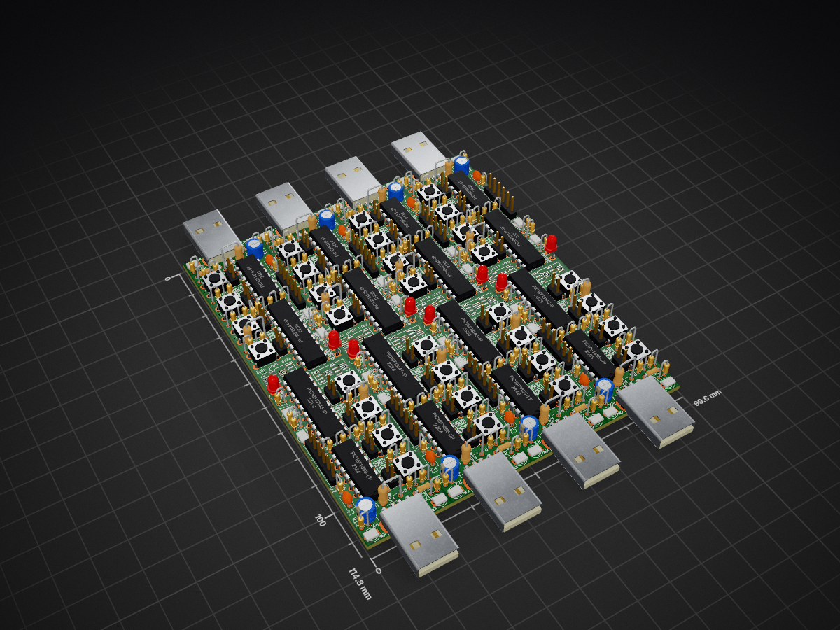
MiniFPGA panel is an open-source printed circuit board by MicrochipTech, from the MicrochipTech/veryVerilog repository on GitHub. It is a 2-layer board of 99.6 × 114.8 mm with 400 parts on 392 nets, routed with 1,952 tracks and 144 vias.
It is built around the PIC16F1455-I/P. Its parts include 168 resistors, 40 diodes, 16 capacitors, 16 ICs and 16 connectors. It belongs with the PIC boards of this library.
veryVerilog enables an easy way to program PICs from family
over a Web Browser without the need to install any software using a PIC as a USB HiD device.
The project is based on 3 parts:
The PCB looks like this and is based on a PIC16F1455 .
The PIC16F1455 needs a custom firmware to perform as ICSP programmer.
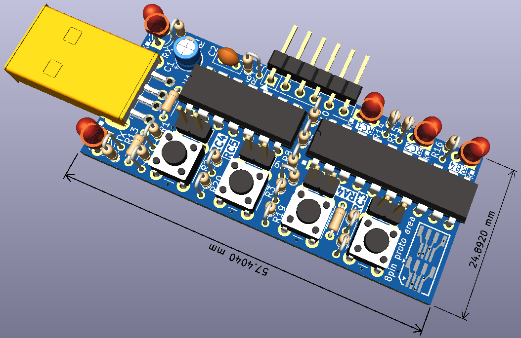
The IC on the left-hand side is the PIC16F1455-I/P and IC on the right-hand side is the miniFPGA (PIC16F13145-I/P) to be programmed.
It is that easy:
Plug the miniFPGA dongle in your computer.
Open the Web Page: https://microchiptech.github.io/veryVerilog.
You will see the veryVerilog Web Page:

Click the button "Connect to Programmer" and select the miniFPGA device:
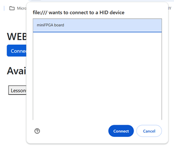
If you have multiple programmers connected, click "identify Programmer" and the LEDs of the connected board will blink for about 2 seconds.
The device is recognized and the Web Page displays information about the connected PIC and the identification of the program already flashed on the device (User Id)

Drag a HEX file on the "Drag and Drop" area and the program will be transfered automatically to the PIC.

Alternatively, you can click the "Browse for HEX file" button to select a HEX file from your file system. This is particularly useful when working with IDEs where you can copy and paste file paths.
Have fun!
After connecting to the programmer, a "Reset Target" button becomes available. Clicking this button will reset the target PIC.
When you connect to a programmer:
This helps in debugging connectivity issues or identifying when an unsupported PIC is connected.
Tip: Click on the UserId display to open a detailed information window showing:
After connecting to the programmer, you can read the entire contents of the target PIC device:
The memory viewer organizes data into collapsible sections:
You can also access previously read memory using the "Show Memory" option without reading the device again. This is useful for comparing data or reviewing what was last read from the device.
The Settings dropdown provides options to customize which memory regions are programmed and whether verification is performed:
Default Behavior:
Customizing Memory Regions:
Click the Settings dropdown to access programming options. You can selectively choose which memory regions to program by checking/unchecking:
Verification:
The veryVerilog web page includes a built-in Serial Terminal for communicating directly with the target PIC over a serial (UART) connection.
Click the "Serial Terminal" tab to open the terminal window:
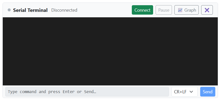
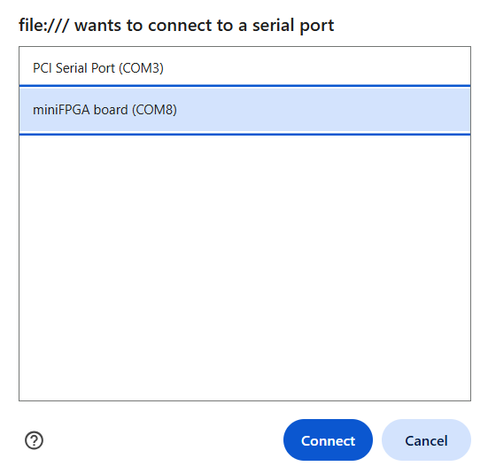
Click the "Connect" button and a browser popup will appear listing the available serial ports on your computer. Select the desired port (e.g., the miniFPGA board) and click Connect:
Once connected, the status indicator turns green and the terminal displays a confirmation message with a timestamp:
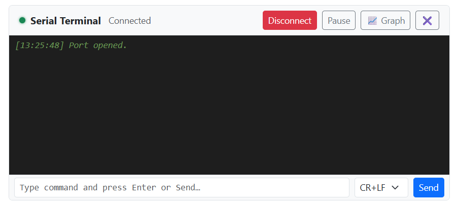
Type a command in the input field at the bottom of the terminal and press Enter or click the "Send" button. Use the line ending dropdown (default: CR+LF) to choose the line termination characters appended to each message.
The toolbar at the top of the terminal provides the following controls:
| Button | Description |
|---|---|
| Connect / Disconnect | Connect to or disconnect from a serial port. The button label changes depending on the connection state. |
| Pause | Pause the terminal output. Incoming data is still received but the display stops scrolling. Click again to resume. |
| Graph | Open a graphing view to plot numeric data received from the serial port in real time (see Graph Mode below). |
| X (Clear Terminal) | Clear all text currently displayed in the terminal window. |
| Hide Terminal | Collapse the serial terminal panel to free up screen space. Click the "Serial Terminal" tab again to reopen it. |
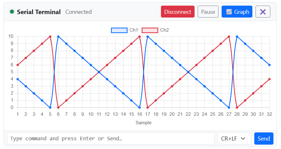
Click the "Graph" button to switch the terminal into a real-time plotting view. The graph plots numeric data received over the serial port in CSV format — each line of text represents one data point in time, with comma-separated values mapping to individual channels.
Expected data format:
The PIC should send an optional header line followed by numeric data lines, all in CSV format terminated by a newline:
header1,header2,header3\n   ← optional: names for each channel
value1,value2,value3\n      ← numeric data (one sample per line)
value1,value2,value3\n
...
The first non-numeric line received is used as the channel names displayed in the graph legend. If no header is sent, channels are automatically named Ch1, Ch2, etc.
Tip: Always send a header line at PIC startup to get meaningful trace names. Without it, UART noise or partial bytes at connection time may produce garbled labels.
Example — single channel (e.g., ADC reading):
ADC
512
523
531
548
Example — multiple channels (e.g., temperature and humidity sensors):
Temperature,Humidity
23.5,65.2
23.6,64.8
23.7,65.0
23.8,64.5
Example C code to send plottable data from a PIC:
// Send header once at startup
printf("ADC,Temperature\r\n");

// Then send data periodically
while (1) {
    printf("%d,%d\r\n", adc_value, temperature);
    __delay_ms(100);
}
Each comma-separated value is plotted as a separate trace on the graph, allowing you to monitor multiple signals simultaneously. The example below shows two channels — one counting up from 0 to 10 and the other counting down from 10 to 0 — plotted in real time:
| Qty | Value | Footprint | References |
|---|---|---|---|
| 144 | 680Ω | Attila:R_Axial_L3.6mm_D1.6mm_P1.90mm_Vertical | R1, R1, R1, R1, R1, R1, R1, R1, R10, R10, R10, R10, R10, R10, R10, R10 +128 |
| 24 | 10kΩ | Resistor_THT:R_Axial_DIN0204_L3.6mm_D1.6mm_P5.08mm_Horizontal | R11, R11, R11, R11, R11, R11, R11, R11, R18, R18, R18, R18, R18, R18, R18, R18 +8 |
| 8 | 1 | TestPoint:TestPoint_Pad_1.5x1.5mm | TP1, TP1, TP1, TP1, TP1, TP1, TP1, TP1 |
| 8 | 2 | TestPoint:TestPoint_Pad_D1.5mm | TP2, TP2, TP2, TP2, TP2, TP2, TP2, TP2 |
| 8 | 3 | TestPoint:TestPoint_Pad_D1.5mm | TP3, TP3, TP3, TP3, TP3, TP3, TP3, TP3 |
| 8 | 4 | TestPoint:TestPoint_Pad_D1.5mm | TP4, TP4, TP4, TP4, TP4, TP4, TP4, TP4 |
| 8 | 470nF | Capacitor_THT:C_Rect_L4.6mm_W2.0mm_P2.50mm_MKS02_FKP02 | C2, C2, C2, C2, C2, C2, C2, C2 |
| 8 | 4µ7F | Capacitor_THT:CP_Radial_D4.0mm_P2.00mm | C1, C1, C1, C1, C1, C1, C1, C1 |
| 8 | 5 | TestPoint:TestPoint_Pad_D1.5mm | TP5, TP5, TP5, TP5, TP5, TP5, TP5, TP5 |
| 8 | 6 | TestPoint:TestPoint_Pad_D1.5mm | TP6, TP6, TP6, TP6, TP6, TP6, TP6, TP6 |
| 8 | 7 | TestPoint:TestPoint_Pad_D1.5mm | TP7, TP7, TP7, TP7, TP7, TP7, TP7, TP7 |
| 8 | 8 | TestPoint:TestPoint_Pad_D1.5mm | TP8, TP8, TP8, TP8, TP8, TP8, TP8, TP8 |
| 8 | 8pin proto area | Attila:8pin_proto | A1, A1, A1, A1, A1, A1, A1, A1 |
| 8 | ICSP_DEBUG_miniFPGA | Connector_PinHeader_2.54mm:PinHeader_1x06_P2.54mm_Horizontal | J2, J2, J2, J2, J2, J2, J2, J2 |
| 8 | LOGO | Attila:MClogoBW_18x4.2mm | REF*, REF*, REF*, REF*, REF*, REF*, REF*, REF* |
| 8 | PIC16F13145-IP | Package_DIP:DIP-20_W7.62mm | U2, U2, U2, U2, U2, U2, U2, U2 |
| 8 | PIC16F1455-I/P | Package_DIP:DIP-14_W7.62mm | U1, U1, U1, U1, U1, U1, U1, U1 |
| 8 | RA4 | Connector_PinHeader_2.54mm:PinHeader_1x02_P2.54mm_Vertical | JP3, JP3, JP3, JP3, JP3, JP3, JP3, JP3 |
| 8 | RA4 | Button_Switch_THT:SW_PUSH_6mm_H5mm | PB3, PB3, PB3, PB3, PB3, PB3, PB3, PB3 |
| 8 | RB4 | LED_THT:LED_D3.0mm | LED5, LED5, LED5, LED5, LED5, LED5, LED5, LED5 |
| 8 | RC1 | LED_THT:LED_D3.0mm | LED3, LED3, LED3, LED3, LED3, LED3, LED3, LED3 |
| 8 | RC2 | LED_THT:LED_D3.0mm | LED4, LED4, LED4, LED4, LED4, LED4, LED4, LED4 |
| 8 | RC3 | Connector_PinHeader_2.54mm:PinHeader_1x02_P2.54mm_Vertical | JP4, JP4, JP4, JP4, JP4, JP4, JP4, JP4 |
| 8 | RC3 | Button_Switch_THT:SW_PUSH_6mm_H5mm | PB4, PB4, PB4, PB4, PB4, PB4, PB4, PB4 |
| 8 | RC4 | Connector_PinHeader_2.54mm:PinHeader_1x02_P2.54mm_Vertical | JP1, JP1, JP1, JP1, JP1, JP1, JP1, JP1 |
| 8 | RC4 | Button_Switch_THT:SW_PUSH_6mm_H5mm | PB1, PB1, PB1, PB1, PB1, PB1, PB1, PB1 |
| 8 | RC5 | Connector_PinHeader_2.54mm:PinHeader_1x02_P2.54mm_Vertical | JP2, JP2, JP2, JP2, JP2, JP2, JP2, JP2 |
| 8 | RC5 | Button_Switch_THT:SW_PUSH_6mm_H5mm | PB2, PB2, PB2, PB2, PB2, PB2, PB2, PB2 |
| 8 | RX | LED_THT:LED_D3.0mm | LED1, LED1, LED1, LED1, LED1, LED1, LED1, LED1 |
| 8 | TX | LED_THT:LED_D3.0mm | LED2, LED2, LED2, LED2, LED2, LED2, LED2, LED2 |
| 8 | USB_B | Connector_USB:USB_A_CNCTech_1001-011-01101_Horizontal | J1, J1, J1, J1, J1, J1, J1, J1 |
MicrochipTech/veryVerilog
Learn Verilog basics the easy way with the world's smallest FPGA.


PostTenebrasLab/PTL-ino
The PTL-ino (“petilino”) is a *uino-compatbile board that is fully made of easily solderable through-hole components.


stonedDiscord/nonSNES
Super Nintendo Entertainment System PAL schematic and board layout


PerMalmberg/IO-Card-G3
This is my custom I/O card, third generation. Main purpose is to serve as an alarm system.

SolderedElectronics/Slider-potentiometer-breakout-hardware-design
Hardware design, BOM, gerbers and 3D files for Slider-potentiometer-breakout designed by Soldered Electronics.
It measures 99.6 × 114.8 mm and has 2 copper layers, 1.6 mm thick.
400 parts, built around the PIC16F1455-I/P. The full list of its parts is on this page, with links to each part's symbol and footprint where PCBKit's library has them.
From the MicrochipTech/veryVerilog repository on GitHub, at the commit this page was made from: the board is PCB/miniFPGA/miniFPGA_panel.kicad_pcb and its schematic PCB/miniFPGA/miniFPGA.kicad_sch. PCBKit opens the board in the browser, with nothing to install.
Its repository states no licence, so its author keeps all rights: ask MicrochipTech before reusing the design.