
2 layers65 × 56 mm
ROVPCB
dakriy/Rosario-ROV
This project is to create a working ROV with features such as live video for the WWU Rosario Beach Marine Laboratory.
24 parts3MIT
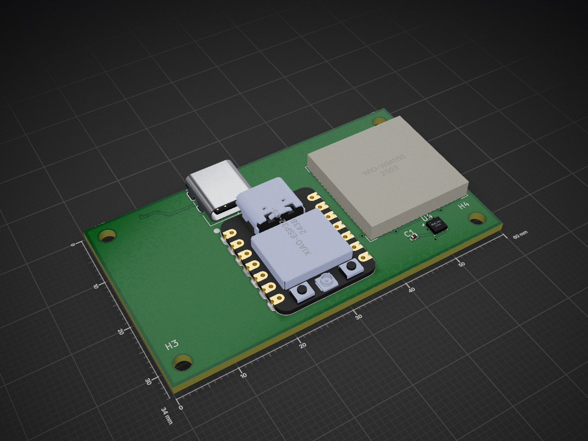
 MetaStrawman/chameleon-mesh-node1
Chameleon Mesh Node — Seeed Meshtastic Build-Off 2026: dual-radio off-grid telemetry + LoRa mesh relay (Wio-WM1110 LoRa/GNSS + XIAO ESP32-C5 + BME280)
Chameleon mesh node v1 is an open-source printed circuit board by MetaStrawman, from the MetaStrawman/chameleon-mesh-node repository on GitHub. It is a 2-layer board of 60 × 34 mm with 9 parts on 9 nets, routed with 203 tracks and 16 vias.
It is built around the BME280, WIO-WM1110 and M2.5. Its parts include 3 ICs, 1 capacitor and 1 connector. It belongs with the radio and wireless boards and the ESP32 and RISC-V boards of this library.

A rugged, dual-radio environmental telemetry node built on the Meshtastic + LoRa stack.
Submission: Seeed Studio Meshtastic Build-Off 2026
Status: Design complete & verified — routed, DRC-clean (0 errors / 0 unconnected; 29 cosmetic silkscreen/DFM warnings), Gerbers exported. Pre-fabrication (first article not yet ordered).
Hardware revision: v1.2
License: Multi-license open source — CERN-OHL-S-2.0 (hardware), GPL-3.0-or-later (Meshtastic firmware variant), MIT (tooling). See LICENSE and NOTICE.md.
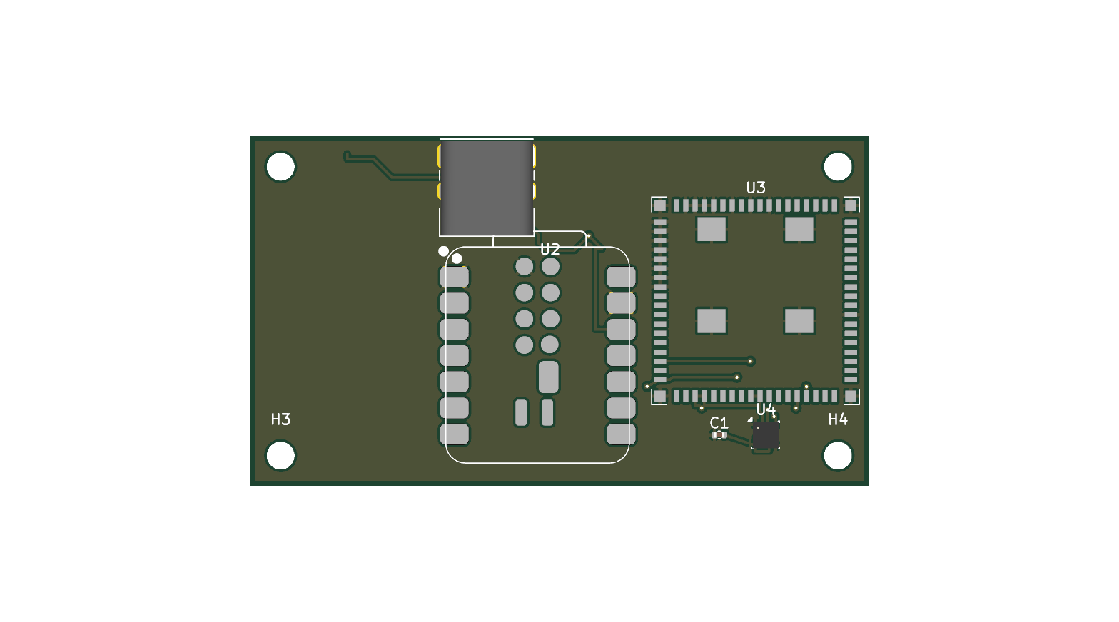
3D render (top). Bottom: assets/chameleon_mesh_node_v1_bottom.png.
The Chameleon Mesh Node is a single-board, USB-powered field appliance for Meshtastic telemetry. It joins a Meshtastic mesh on sub-GHz LoRa for resilient long-range messaging, reads local environment with an on-board sensor, and exposes a Wi-Fi / BLE side-channel for short-range provisioning and bulk-data offload.
Designed as a compact, regenerable two-radio Meshtastic reference board.
Most off-the-shelf Meshtastic nodes pick one path: a LoRa-only board that needs a phone to provision, or a Wi-Fi-only "smart sensor" that needs an AP within range. Neither survives a real off-grid deployment where the closest infrastructure is hours away.
This board pairs two complementary radio subsystems on one PCB:
| Subsystem | Role | Module |
|---|---|---|
| Long-range mesh | Meshtastic LoRa + GNSS time-sync + Wi-Fi scan for opportunistic uplink | Seeed Wio-WM1110 (Semtech LR1110 + Nordic nRF52840) |
| Local-area + provisioning | Wi-Fi 6 / BLE 5 / 802.15.4 for setup, OTA, and bulk data offload to a passing operator's phone | Seeed XIAO ESP32-C5 |
Both radios cohabit one 60×34 mm 2-layer board, with explicit RF zoning and a shared ground pour designed to keep mutual desense within acceptable limits for an environmental-sensing-class duty cycle.
| Dimensions | 60 × 34 mm, 2-layer FR-4 |
| MCU | Nordic nRF52840 (Meshtastic firmware host) + Espressif ESP32-C5 (companion) |
| Radios | Semtech LR1110 (sub-GHz LoRa, GNSS, passive Wi-Fi scan); Wi-Fi 6 / BLE 5 / 802.15.4 |
| Power input | USB-C 5 V (XIAO ESP32-C5 onboard port) |
| Environmental sensor | Bosch BME280 (temperature, humidity, barometric pressure, I²C) |
| Operating temperature | -20 °C to +60 °C (designed; pending environmental test) |
chameleon_mesh_node/
├── README.md                — this file
├── LICENSE                  — multi-license map (see also LICENSES/, NOTICE.md)
├── LICENSES/                — full license texts (CERN-OHL-S-2.0, GPL-3.0, MIT)
├── NOTICE.md                — third-party attribution
├── Makefile                 — `make demo` / erc / drc / gerbers / clean targets
├── scripts/demo.sh          — one-command launch demo (design reveal)
├── assets/                  — 3D renders
├── docs/
│   ├── architecture.md      — block diagram, radio zoning, antenna feeds
│   ├── build-guide.md       — BOM, assembly notes, first-power-on checklist
│   └── power-design.md      — USB-C power input and module power tree
├── hardware/
│   ├── kicad/               — KiCad 10 project (schematic, PCB, footprints, gerber zips)
│   ├── gerbers/             — extracted v1.2 Gerbers + Excellon drill (fab-ready)
│   └── scripts/             — Python composers that regenerate schematic + PCB from source
├── firmware/                — Meshtastic nRF52840 variant (variant.h + platformio.ini) + ESP32-C5 stub
└── enclosure/cad/           — 3D-printable case (planned, post-fab)
The KiCad project is fully regenerable: python3 hardware/scripts/build_schematic.py rebuilds the schematic from the Python composer, and python3 hardware/scripts/build_pcb.py rebuilds the pre-placed PCB. You can wipe the .kicad_* files and reproduce the design from source.
make demoRuns the one-command, non-destructive launch demo (design reveal): the Python
generators compile, the schematic passes ERC, the PCB DRC connectivity check
runs, and a fresh Gerber/drill fabrication package is exported to a throwaway
build/ directory. No device, no servers, no GUI. Requires python3 and
kicad-cli (KiCad 10.x); make help lists the individual targets
(compile, erc, drc, gerbers, clean).
The Chameleon Mesh Node is a Meshtastic node. The Nordic nRF52840 core of the Wio-WM1110 runs the Meshtastic firmware; the Semtech LR1110 is its sub-GHz LoRa radio (plus GNSS time-sync and passive Wi-Fi scan). It joins a Meshtastic mesh, announces itself, relays messages, and publishes its BME280 environmental readings as Meshtastic telemetry — provisioned over BLE with the standard Meshtastic mobile app.
Because the base board (Seeed Wio-WM1110 / nRF52840 + LR1110) is already supported
upstream, this project ships as an incremental hardware variant, not a new port.
The board-specific deltas (BME280 at I²C 0x76, an ESP32-C5 companion-wake GPIO)
are captured in firmware/variant.h +
firmware/platformio.ini, layered on the upstream
Wio-WM1110 build environment. See firmware/README.md.
docs/design-rationale.md). Verified with kicad-cli pcb drc --severity-error (KiCad 10.0.3), which reads the scoped custom rule in hardware/kicad/chameleon_mesh_node_v1.kicad_dru.hardware/gerbers/).USB_C_Receptacle_GCT_USB4085 land pattern places its 0.70 mm through-hole pads on 0.85 mm pitch, an inherent 0.15 mm pad-to-pad gap that the 0.20 mm Default-netclass clearance flags. Rather than shrink the pads (which would thin the annular ring and weaken a mechanically-cycled connector joint), the manufacturer land pattern is preserved and design intent is expressed with a scoped custom design rule (hardware/kicad/chameleon_mesh_node_v1.kicad_dru) that sets a 0.15 mm clearance for J1's own pads only — the 0.20 mm rule still governs everywhere else. The 15th was a real GND↔+3V3 track crossing beside U4 (the sensor), rerouted by dropping the GND leg onto the B.Cu ground plane with two vias. Netlist unchanged; F/B copper and drill re-exported.The board is design-complete and verified — schematic + ERC clean, RF-zoned placement, routing and ground pour done, DRC clean (0 errors / 0 unconnected), and the full fabrication package (gerbers, drill, BOM, placement, schematic PDF, 3D renders) is exported and committed. This revision is fab-ready.
Next: first-article prototype, board bring-up (power smoke test, Meshtastic flash over SWD, mesh-join test), deep-sleep current measurement, upstreaming the Meshtastic variant, and an enclosure design.
Multi-license open source — see LICENSE for the per-component map and
LICENSES/ for full texts. Hardware: CERN-OHL-S-2.0. Meshtastic
firmware variant: GPL-3.0-or-later. Tooling/generators: MIT. Third-party
components retain their upstream licenses (NOTICE.md).
See repository issues for design questions, build reports, or fork notifications.
| Qty | Value | Footprint | References |
|---|---|---|---|
| 4 | M2.5 | ChameleonMeshNode_Custom:MountingHole_M2.5 | H1, H2, H3, H4 |
| 1 | 100nF | C_0402_1005Metric | C1 |
| 1 | BME280 | Package_LGA:Bosch_LGA-8_2.5x2.5mm_P0.65mm_ClockwisePinNumbering | U4 |
| 1 | USB-C Power+Data | Connector_USB:USB_C_Receptacle_GCT_USB4085 | J1 |
| 1 | Wio-WM1110 | ChameleonMeshNode_Custom:Wio_WM1110_LGA80 | U3 |
| 1 | XIAO-ESP32-C5-SMD | Seeed_XIAO:XIAO-ESP32-C5-SMD | U2 |
dakriy/Rosario-ROV
This project is to create a working ROV with features such as live video for the WWU Rosario Beach Marine Laboratory.

Mehdi-Ldj/lora-ble-sensor-node
Off-grid LoRa/BLE sensor node — 868 MHz LoRa, 2.4 GHz BLE, solar/LiFePO4

Spirit532/studio_mic
A simple, easy to build preamplifier for any true condenser capsule, to make a condenser microphone


gmcn42/clumsyMIDI
A THT-only Raspberry Pi expansion board containing a MIDI interface, DAC, and OLED display

DvidMakesThings/HW_PDNode-600-Pro
The PDNode-600 is a professional-grade, 600W USB Power Delivery Unit designed specifically for compact 10-inch rack systems, targeting embedded developers, homelab enthusiasts, test benches, and smart infrastructure.


It measures 60 × 34 mm and has 2 copper layers, 1.6 mm thick.
9 parts, built around the BME280, WIO-WM1110 and M2.5. The full list of its parts is on this page, with links to each part's symbol and footprint where PCBKit's library has them.
From the MetaStrawman/chameleon-mesh-node repository on GitHub, at the commit this page was made from: the board is hardware/kicad/chameleon_mesh_node_v1.kicad_pcb and its schematic hardware/kicad/chameleon_mesh_node_v1.kicad_sch. PCBKit opens the board in the browser, with nothing to install.
Its repository states no licence, so its author keeps all rights: ask MetaStrawman before reusing the design.