
2 layers25.9 × 17 mm
SnapVCC
electronut/ElectronutLabs-snapVCC
A tiny 3.3 V / 5 V voltage regulator that snaps right on top of a 9 volt battery.
45 parts77
 MadhuFire/HardwarePCBDesign_InternWorks
The converter is capable of: - Accepting variable input voltage - Automatically operating in both buck and boost modes - Providing regulated 5V output - Delivering up to approximately 800mA output current
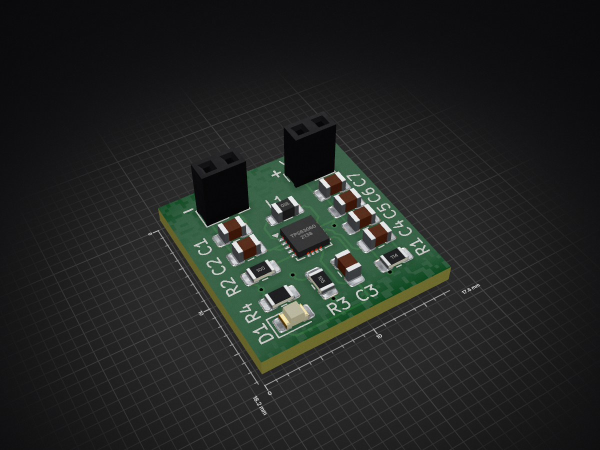
BuckBoost 1 is an open-source printed circuit board by MadhuFire, from the MadhuFire/HardwarePCBDesign_InternWorks repository on GitHub. It is a 2-layer board of 17.6 × 18.2 mm with 16 parts on 9 nets, routed with 105 tracks and 5 vias.
It is built around the TPS63060DSC. Its parts include 7 capacitors, 4 resistors, 1 IC, 1 diode and 1 inductor.
This project is a custom designed DC-DC buck-boost converter PCB based on the TPS63060 power management IC.
The PCB was designed completely in KiCad as a learning and practical hardware implementation project to understand PCB design workflows, routing techniques, DRC validation, and manufacturing file generation.
The converter is capable of:
| Parameter | Value |
|---|---|
| Input Voltage | 2.5V to 12V |
| Output Voltage | 5V |
| Output Current | Up to ~800mA |
| Converter Type | Buck-Boost |
| PCB Software | KiCad |
The TPS63060 dynamically switches between buck and boost conversion modes depending on the input voltage.
| Component | Description |
|---|---|
| TPS63060 | Buck-Boost Converter IC |
| L1 | 1uH Inductor |
| C1, C2 | Input Capacitors |
| C5, C6, C7 | Output Capacitors |
| R1, R2, R3, R4 | Feedback and control resistors |
| D1 | LED Indicator |
Performed Design Rule Check (DRC) to verify:
All DRC errors and warnings were resolved successfully.
One of the biggest challenges during this project was routing around the compact TPS63060 package while maintaining:
Initially many routing and clearance issues occurred during PCB design.
After debugging and understanding KiCad routing behavior, grid settings, net classes, and DRC constraints, the PCB was completed successfully.
This project helped in understanding real-world PCB routing challenges and hardware debugging workflows.
Manufacturing files were generated successfully for PCB fabrication:
These files are ready for PCB manufacturers such as:
KiCad 3D Viewer was used to:
✅ Schematic Completed
✅ PCB Layout Completed
✅ Routing Completed
✅ DRC Passed
✅ Ground Plane Added
✅ Gerber Files Generated
✅ Drill Files Generated
✅ 3D Visualization Completed
This repository includes:
This project helped transition from learning electronics theory to understanding practical hardware implementation and real PCB design workflows.
Along with this project, I also started gaining industry exposure through a hardware and PCB design internship, which is helping me understand:
Still learning, building, debugging, and improving every day 🚀
Madhukumaran
1st YEAR VLSI
| Qty | Value | Footprint | References |
|---|---|---|---|
| 3 | 22uF | Capacitor_SMD:C_0805_2012Metric_Pad1.18x1.45mm_HandSolder | C5, C6, C7 |
| 2 | 10uF 16V | Capacitor_SMD:C_0805_2012Metric_Pad1.18x1.45mm_HandSolder | C1, C2 |
| 2 | 1M | Resistor_SMD:R_0805_2012Metric_Pad1.20x1.40mm_HandSolder | R2, R3 |
| 1 | 0.1uF | Capacitor_SMD:C_0805_2012Metric_Pad1.18x1.45mm_HandSolder | C3 |
| 1 | 10pF | Capacitor_SMD:C_0805_2012Metric_Pad1.18x1.45mm_HandSolder | C4 |
| 1 | 111k | Resistor_SMD:R_0805_2012Metric_Pad1.20x1.40mm_HandSolder | R1 |
| 1 | 1uH | Inductor_SMD:L_0805_2012Metric_Pad1.05x1.20mm_HandSolder | L1 |
| 1 | 430-5% | Resistor_SMD:R_0805_2012Metric_Pad1.20x1.40mm_HandSolder | R4 |
| 1 | LED | LED_SMD:LED_0805_2012Metric_Pad1.15x1.40mm_HandSolder | D1 |
| 1 | TPS63060 | Package_SON:Texas_S-PWSON-N10_ThermalVias | U2 |
| 1 | Vin | Connector_PinSocket_2.00mm:PinSocket_1x02_P2.00mm_Vertical | Vin |
| 1 | Vout | Connector_PinSocket_2.00mm:PinSocket_1x02_P2.00mm_Vertical | Vout |
electronut/ElectronutLabs-snapVCC
A tiny 3.3 V / 5 V voltage regulator that snaps right on top of a 9 volt battery.

samyyy2311/CassetteCat
A music player for Android. Plays your own files, Jellyfin and Navidrome/Subsonic servers, and internet radio, with synced lyrics, an equalizer, Android Auto and a Listening Record. No account or tracking.

0Zane/Nomad
One Adventure - One device,Nomad is a custom outdoor mobile device built around the ESP32-S3. It is designed for explorers, researchers, and outdoor enthusiasts who need reliable positioning, long-range communication…


PREDICT-EPFL/RoboCape
This repository is dedicated to a Beaglebone cape extension developped at EPFL in the Automatic Control Laboratory.


mpkendall/Tiny4FSK-Ecosystem
Set of expansion boards, sensor breakouts, and additional modules to operate with the Tiny4FSK tracking system.
It measures 17.6 × 18.2 mm and has 2 copper layers, 1.6 mm thick.
16 parts, built around the TPS63060DSC. The full list of its parts is on this page, with links to each part's symbol and footprint where PCBKit's library has them.
From the MadhuFire/HardwarePCBDesign_InternWorks repository on GitHub, at the commit this page was made from: the board is Regulator_TPS63060IC/BuckBoost_1.kicad_pcb and its schematic Regulator_TPS63060IC/BuckBoost_1.kicad_sch. PCBKit opens the board in the browser, with nothing to install.
Its repository states no licence, so its author keeps all rights: ask MadhuFire before reusing the design.