2 layers80.5 × 62 mm
PCB course
seankyer/QuickSig
A signal generator circuit completed as part of a PCB course at UBC
73 parts

 Jmanicom/ELAB-Signal-Generator
A square wave generator with adjustable frequency, gain, and offset control. Designed as a part of UBC's ELAB PCB design course.
Signal Generator is an open-source printed circuit board by Jmanicom, from the Jmanicom/ELAB-Signal-Generator repository on GitHub, published under the CERN-OHL-S-2.0 licence. It is a 2-layer board of 55.6 × 54.8 mm with 72 parts on 33 nets, routed with 321 tracks and 77 vias.
It is built around the AD8039ARZ, LM7805MP and MAX889SESA+, with the NE555D and DMN10H700S-7 among its other parts. Its parts include 20 resistors, 19 capacitors, 4 ICs, 1 diode and 1 transistor.


A square wave generator with adjustable frequency, gain, and offset control. Designed as a part of UBC's ELAB PCB design course.
KiCad, Analog Circuit Design, Hand Soldering, Testing/Validation
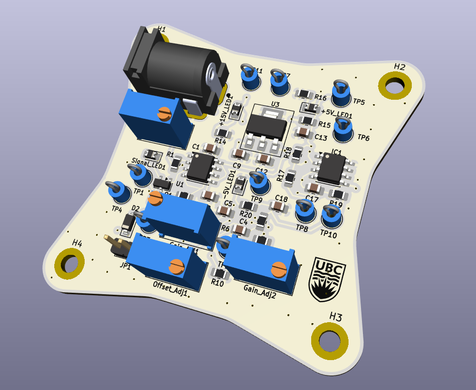
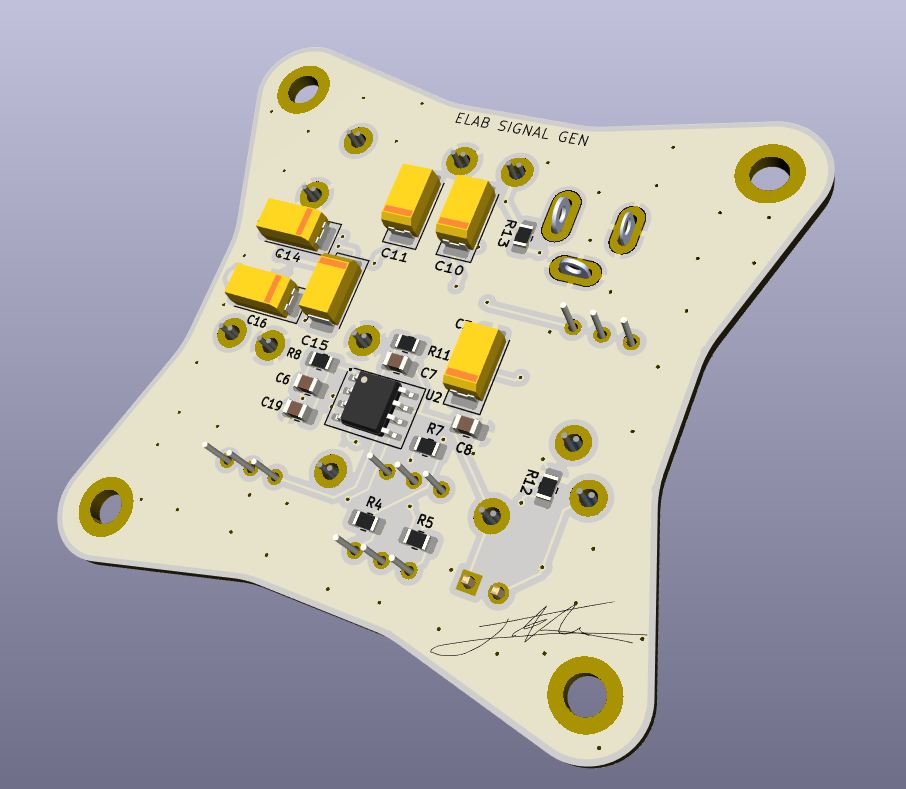
The design for this signal generator is not complex, this is because it's main purpose was to provide an opportunity to design and assemble a PCB from the start to finish of the production cycle. This included schematic capture, component/footprint library creation, component layout, laying traces, and laying polygon pours. In the second stage of the course, we received our boards and components and assembled them using hand soldering, and tested them using an oscilloscope to view our signals and test the various adjustments.
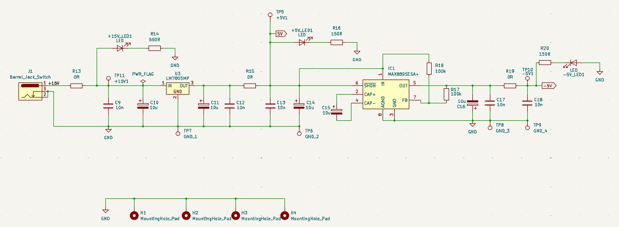
The signal generator utilizes +/-5V rails to be able produce a maximum of a 10V peak-to-peak signal. 15V comes from a barrel jack connections from a wall adapter, which is then regulated using the LM7805 to drop to it to +5V. This rail then feeds into the MAX889 that produces the complimentary -5V rail. Output capacitors are used to help with input noise, and output voltage ripple.
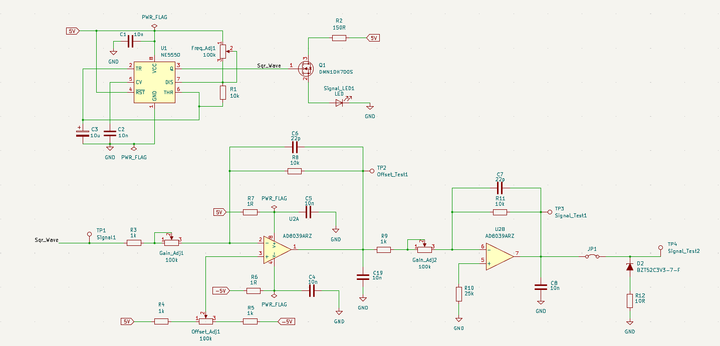
The square wave signal is generated by the NE555, that includes a frequency adjust potentiometer. This signal is then fed to the AD8039 with two amplifier stages to control gain and offset respectively. Additional bypass capacitors are placed on the op-amps power rails to help with further noise reduction and to help stabilize voltage. Finally, a 3.3V peak-limiter zener diode is placed on the output which can be engaged with the use of a jumper.
With this being my first attempt at PCB design, there is room for improvement with my traces decisions component placement. With this project, we were constrained on the size of board that we could use, additionally, I wanted to make a unique shape for my board that tends to be a popular shape for small desings that need to be mounted.
The large 1206 capacitors were placed on the back side of the board as they are quite bulky and left very little room for other components on the board. This board features 2-layers with ground pours on each layer, as well as stitching vias to help further with noise.
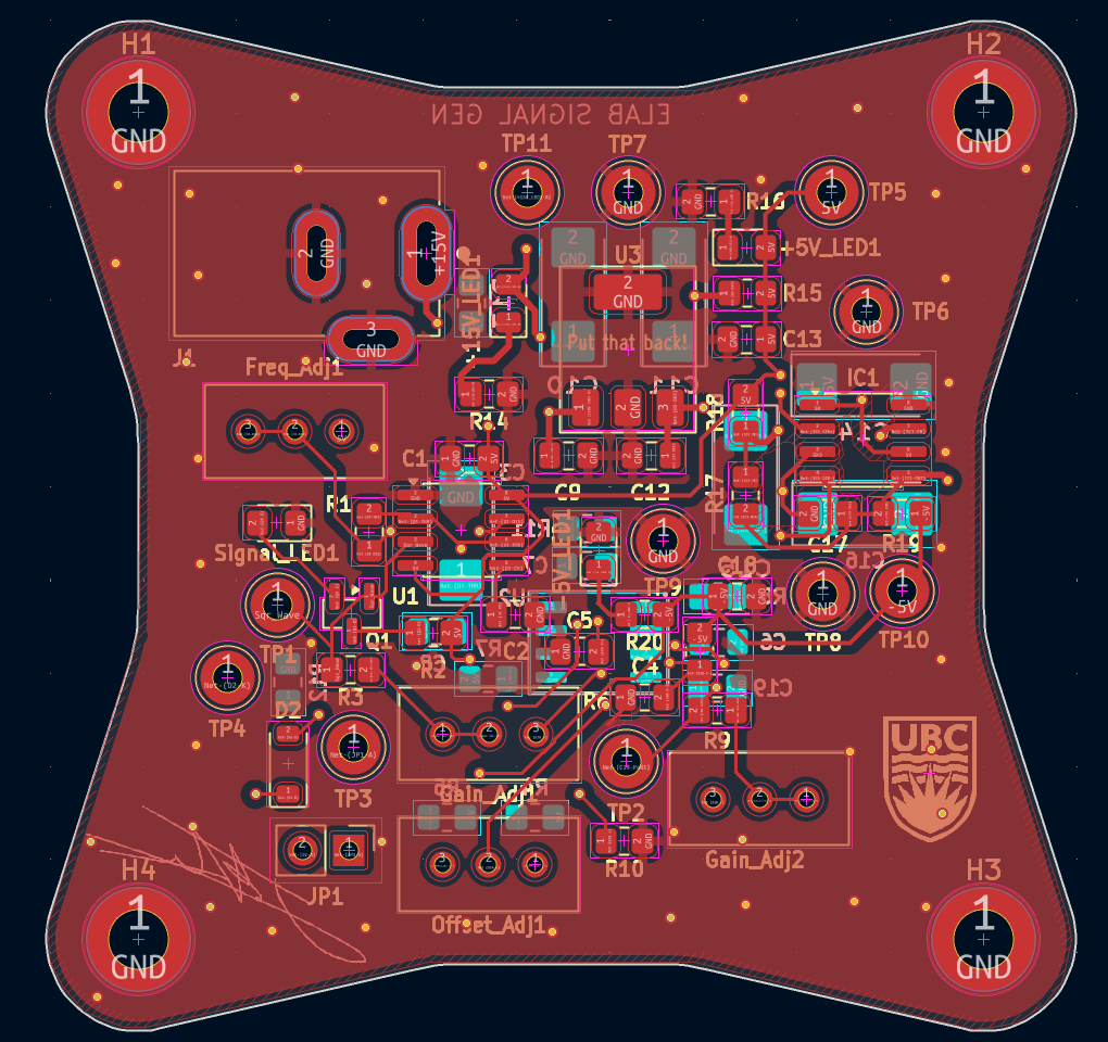
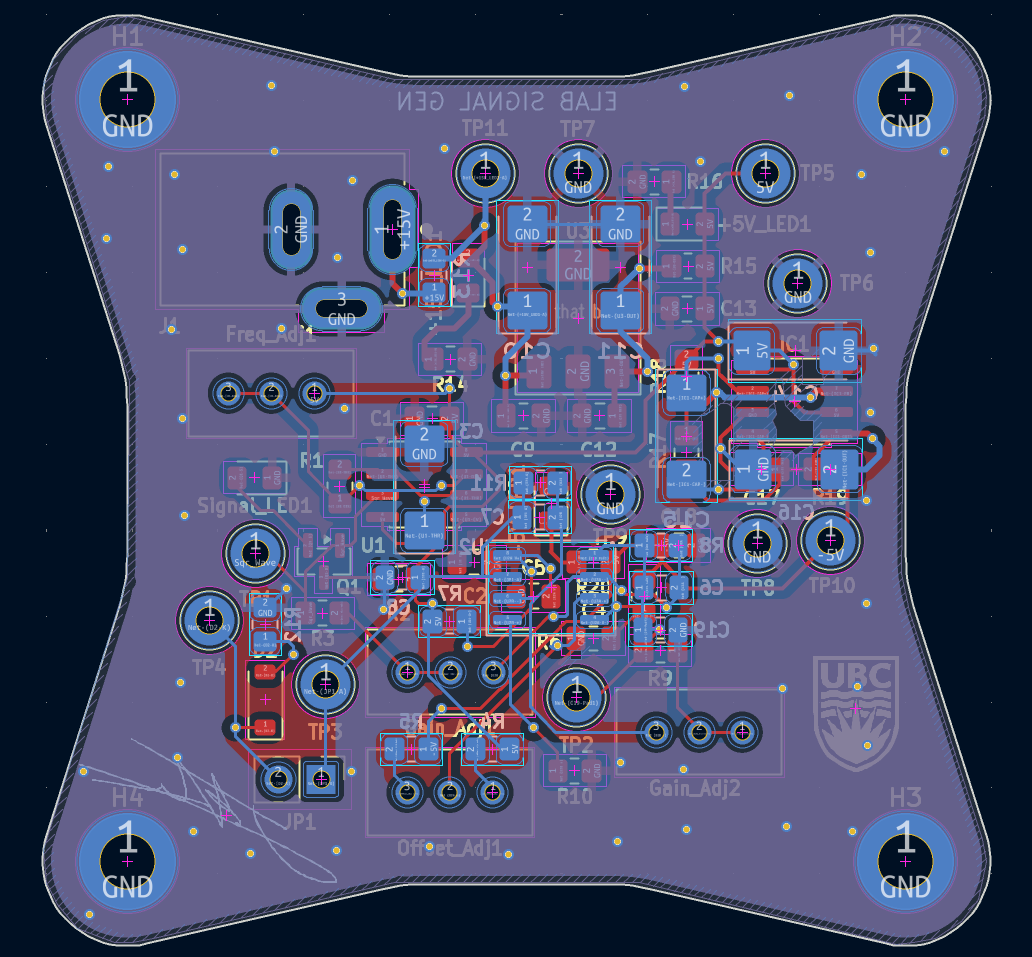
| Qty | Value | Footprint | References |
|---|---|---|---|
| 11 | 10n | Capacitor_SMD:C_0805_2012Metric_Pad1.18x1.45mm_HandSolder | C1, C2, C4, C5, C8, C9, C12, C13, C17, C18, C19 |
| 6 | 10u | Capacitor_Tantalum_SMD:CP_EIA-6032-28_Kemet-C_HandSolder | C3, C10, C11, C14, C15, C16 |
| 4 | 100k | Potentiometer_THT:Potentiometer_Bourns_3296W_Vertical | Freq_Adj1, Gain_Adj1, Gain_Adj2, Offset_Adj1 |
| 4 | 1k | Resistor_SMD:R_0805_2012Metric_Pad1.20x1.40mm_HandSolder | R3, R4, R5, R9 |
| 4 | LED | Diode_SMD:D_0805_2012Metric_Pad1.15x1.40mm_HandSolder | -5V_LED1, +5V_LED1, +15V_LED1, Signal_LED1 |
| 4 | MountingHole_Pad | MountingHole:MountingHole_3.2mm_M3_DIN965_Pad | H1, H2, H3, H4 |
| 3 | 0R | Resistor_SMD:R_0805_2012Metric_Pad1.20x1.40mm_HandSolder | R13, R15, R19 |
| 3 | 10k | Resistor_SMD:R_0805_2012Metric_Pad1.20x1.40mm_HandSolder | R1, R8, R11 |
| 3 | 150R | Resistor_SMD:R_0805_2012Metric_Pad1.20x1.40mm_HandSolder | R2, R16, R20 |
| 2 | 100k | Resistor_SMD:R_0805_2012Metric_Pad1.20x1.40mm_HandSolder | R17, R18 |
| 2 | 1R | Resistor_SMD:R_0805_2012Metric_Pad1.20x1.40mm_HandSolder | R6, R7 |
| 2 | 22p | Capacitor_SMD:C_0805_2012Metric_Pad1.18x1.45mm_HandSolder | C6, C7 |
| 2 | LOGO | LOGO | G***, G*** |
| 1 | +15V1 | TestPoint:TestPoint_Loop_D2.54mm_Drill1.5mm_Beaded | TP11 |
| 1 | +5V1 | TestPoint:TestPoint_Loop_D2.54mm_Drill1.5mm_Beaded | TP5 |
| 1 | -5V1 | TestPoint:TestPoint_Loop_D2.54mm_Drill1.5mm_Beaded | TP10 |
| 1 | 10R | Resistor_SMD:R_0805_2012Metric_Pad1.20x1.40mm_HandSolder | R12 |
| 1 | 25k | Resistor_SMD:R_0805_2012Metric_Pad1.20x1.40mm_HandSolder | R10 |
| 1 | 650R | Resistor_SMD:R_0805_2012Metric_Pad1.20x1.40mm_HandSolder | R14 |
| 1 | AD8039ARZ | PCM_Package_SO_AKL:SO-8_3.9x4.9mm_P1.27mm | U2 |
| 1 | BZT52C3V3-7-F | Diode_SMD:D_SOD-123 | D2 |
| 1 | Barrel_Jack_Switch | Signal-Generator_Footprints:CUI_PJ-002A | J1 |
| 1 | DMN10H700S | Package_TO_SOT_SMD:SOT-23 | Q1 |
| 1 | GND_1 | TestPoint:TestPoint_Loop_D2.54mm_Drill1.5mm_Beaded | TP7 |
| 1 | GND_2 | TestPoint:TestPoint_Loop_D2.54mm_Drill1.5mm_Beaded | TP6 |
| 1 | GND_3 | TestPoint:TestPoint_Loop_D2.54mm_Drill1.5mm_Beaded | TP8 |
| 1 | GND_4 | TestPoint:TestPoint_Loop_D2.54mm_Drill1.5mm_Beaded | TP9 |
| 1 | Jumper_2_Bridged | Connector_PinHeader_2.54mm:PinHeader_1x02_P2.54mm_Vertical | JP1 |
| 1 | LM7805MP | PCM_Package_TO_SOT_SMD_AKL:SOT-223-3_TabPin2 | U3 |
| 1 | MAX889SESA+ | Package_SO:SOIC-8_3.9x4.9mm_P1.27mm | IC1 |
| 1 | NE555D | Package_SO:SOIC-8_3.9x4.9mm_P1.27mm | U1 |
| 1 | Offset_Test1 | TestPoint:TestPoint_Loop_D2.54mm_Drill1.5mm_Beaded | TP2 |
| 1 | Signal1 | TestPoint:TestPoint_Loop_D2.54mm_Drill1.5mm_Beaded | TP1 |
| 1 | Signal_Test1 | TestPoint:TestPoint_Loop_D2.54mm_Drill1.5mm_Beaded | TP3 |
| 1 | Signal_Test2 | TestPoint:TestPoint_Loop_D2.54mm_Drill1.5mm_Beaded | TP4 |
seankyer/QuickSig
A signal generator circuit completed as part of a PCB course at UBC


stefantquach/steDAC
Open source audio DAC project based on the ES9038Q2M DAC from ESS. Still WIP


CosmicPi/CosmicPiV1.7PCB
PCB for Version 1.7 of the Cosmic Pi Hardware. Incremental changes from V1.6. This design is licensed under the CERN OHL V1.2
It measures 55.6 × 54.8 mm and has 2 copper layers, 1.6 mm thick.
72 parts, built around the AD8039ARZ, LM7805MP, MAX889SESA+ and NE555D. The full list of its parts is on this page, with links to each part's symbol and footprint where PCBKit's library has them.
From the Jmanicom/ELAB-Signal-Generator repository on GitHub, at the commit this page was made from: the board is SCH-PCB/Signal Generator.kicad_pcb and its schematic SCH-PCB/Power_Supply.kicad_sch. PCBKit opens the board in the browser, with nothing to install.
Its repository publishes it under the CERN-OHL-S-2.0 licence: you may reuse it on that licence's terms (keep the author's notice, and for a copyleft licence share your changes alike).