


2 layers63.2 × 85 mm
Badge blob
HeyPCB/badge-blob
Blob, the social battery badge: The name badge that tells people whether to come say hi. KiCad 10, heypcb.ai merch.
18 partsCERN-OHL-S-2.0

 HeyPCB/ruler-dino
Ruler Dino: The bench ruler that measures, sizes screws and tests your wires. KiCad 10, heypcb.ai merch.
Ruler dino is an open-source printed circuit board by HeyPCB, from the HeyPCB/ruler-dino repository on GitHub, published under the CERN-OHL-S-2.0 licence. It is a 2-layer board of 156 × 55.9 mm with 13 parts on 5 nets, routed with 42 tracks and 9 vias.
It is built around the CL21A106KAYNNNE, 3034TR and M2.5, with the KT-0603R among its other parts. Its parts include 2 resistors, 1 capacitor and 1 diode.


The bench ruler that measures, sizes screws and tests your wires.
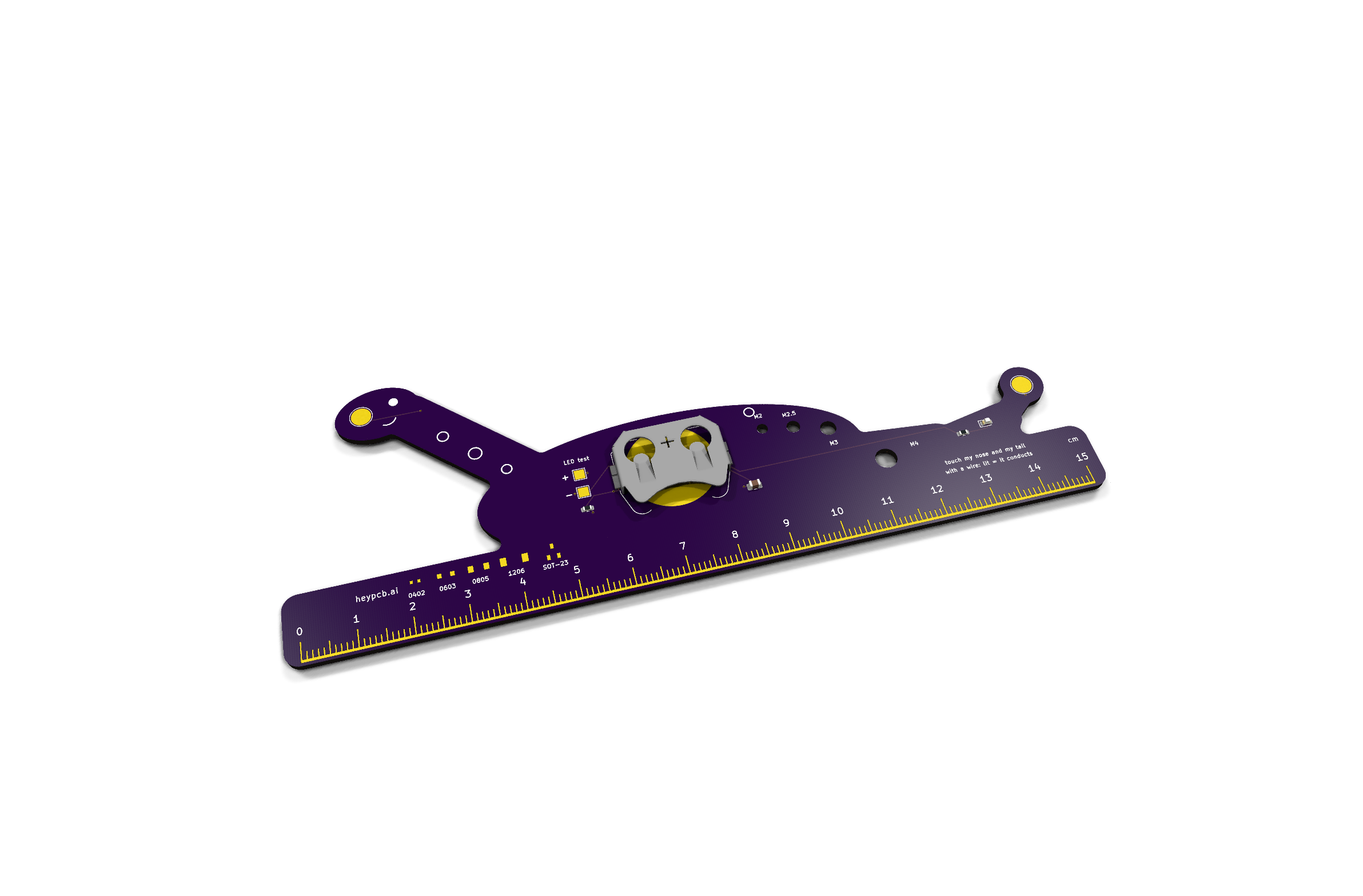
Ruler Dino is a 15 cm workbench ruler shaped like a long-necked dinosaur. Gold ENIG millimetre ticks run along its straight bottom edge; gold land patterns size 0402-1206 passives and SOT-23 parts; drilled holes size M2-M4 screws. A CR2032 in its belly runs an LED tester and a continuity tester: anything that conducts between its gold nose and its gold tail club lights its tail light. The back carries a resistor colour code and an inch scale. There is no MCU.
| Layers | Size | Parts | Nets | Connections routed | Vias | ERC errors | DRC errors / unconnected / parity | BOM @100 |
|---|---|---|---|---|---|---|---|---|
| 2 | 156.1 x 56.0 mm | 9 (+4 pads) | 5 | 10 -> 0 open | 9 | 0 | 0 / 0 / 0 | $0.48 |
Not fabricated, assembled or powered yet. Every number on this page is measured by KiCad 10.0.6 on
the files in this repository (report.json, measured.json) or read
from the live JLC/LCSC catalogue (bom_cost.json).
| Spec, power budget, BOM | SPEC.md |
| Store copy | STORE_COPY.md |
| KiCad 10 project | kicad/ |
| Gerbers, drill, BOM, CPL, STEP, schematic PDF | fab/ |
| Firmware | none: no MCU on this board |
| Renders | front, back, hero, Circuit World thumbnail |
| Brief and generator | design/ |
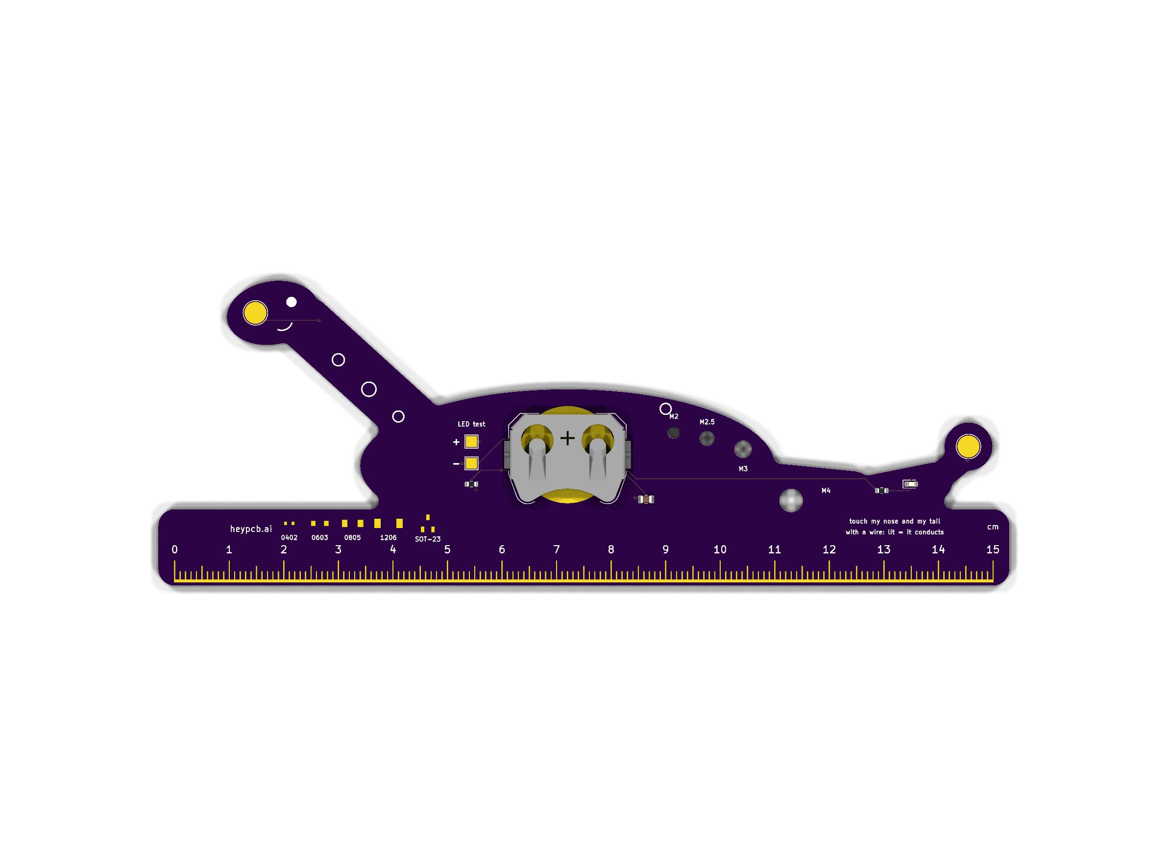
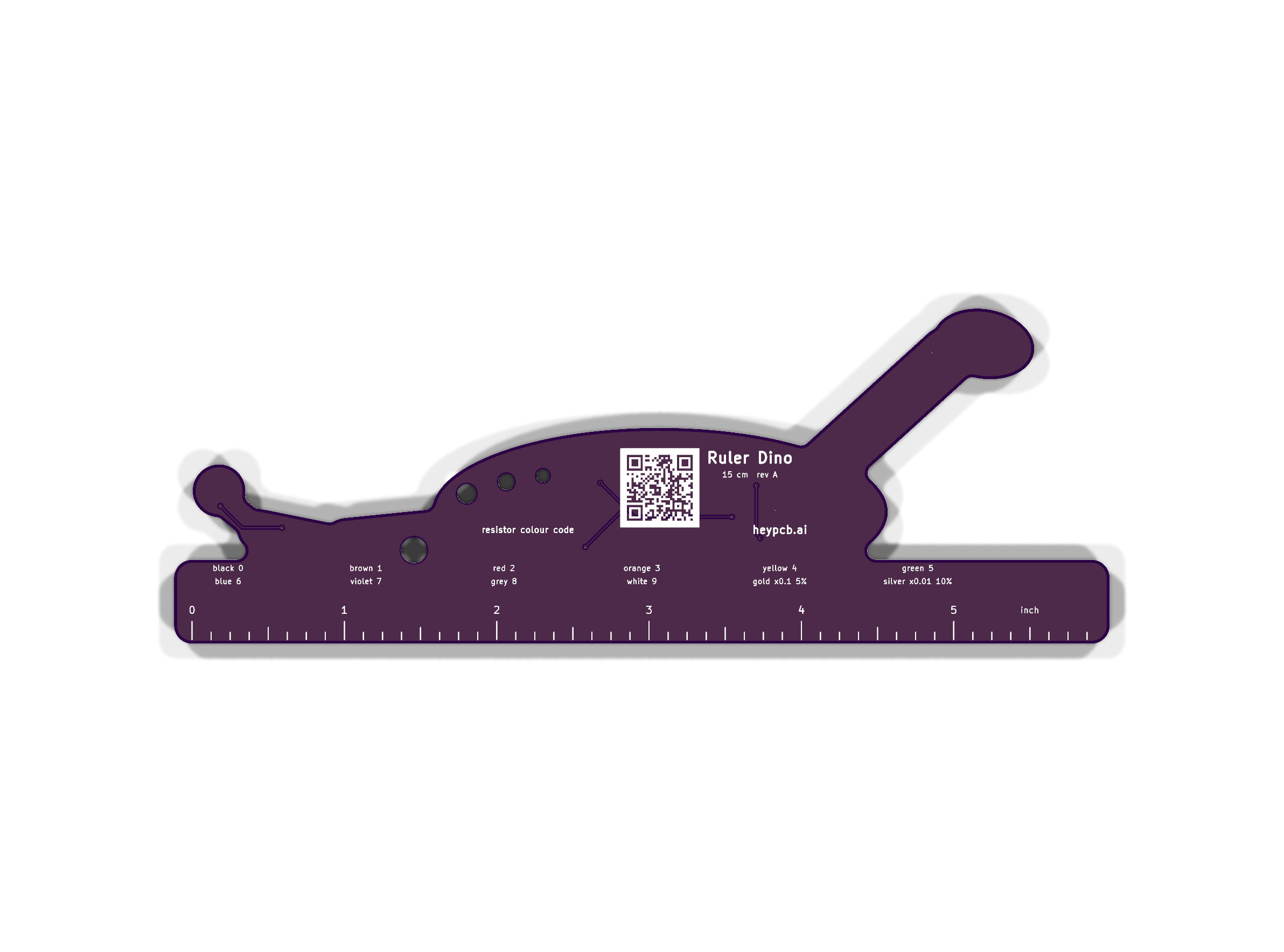
Purple solder mask, White silkscreen, ENIG copper finish, 1.6 mm FR4, top-side SMT assembly. The gold art is bare copper under a mask opening (ENIG), drawn with its own keep-out so no track runs under it. The QR code on the back opens https://heypcb.ai/world/b/9077794f93d5.
Designed with the HeyPCB method on KiCad 10.0.6, headless, by the heypcb-kicad pipeline: a written
brief composed from reusable circuit blocks, every pin from KiCad's own symbol library, every part bound
to an LCSC number from a dated catalogue read, then ERC, a netlist round trip, locked placement,
Freerouting 2.4.1, pours, silkscreen and board art, DRC with schematic parity, DFM and a fab gate,
each stage gated by a measurement. design/make_brief.py regenerates the brief (outline, part
locks and art) from code.
Part of the heypcb.ai merch collection.
Hardware: CERN-OHL-S v2. KiCad's symbol, footprint and 3D libraries used in the design are CC-BY-SA 4.0 with the KiCad library exception.
| Qty | Value | Footprint | References |
|---|---|---|---|
| 1 | 100 | Resistor_SMD:R_0603_1608Metric | R2 |
| 1 | 10uF | Capacitor_SMD:C_0805_2012Metric | C1 |
| 1 | 220 | Resistor_SMD:R_0603_1608Metric | R1 |
| 1 | CR2032 | Battery:BatteryHolder_Keystone_3034_1x20mm | BT1 |
| 1 | LED+ | TestPoint:TestPoint_Pad_2.0x2.0mm | TP3 |
| 1 | LED- | TestPoint:TestPoint_Pad_2.0x2.0mm | TP4 |
| 1 | M2 | MountingHole:MountingHole_2.2mm_M2 | H1 |
| 1 | M2.5 | MountingHole:MountingHole_2.7mm_M2.5 | H2 |
| 1 | M3 | MountingHole:MountingHole_3.2mm_M3 | H3 |
| 1 | M4 | MountingHole:MountingHole_4.3mm_M4 | H4 |
| 1 | PROBE_A | TestPoint:TestPoint_Pad_D4.0mm | TP1 |
| 1 | PROBE_B | TestPoint:TestPoint_Pad_D4.0mm | TP2 |
| 1 | Red | LED_SMD:LED_0603_1608Metric | D1 |
HeyPCB/badge-blob
Blob, the social battery badge: The name badge that tells people whether to come say hi. KiCad 10, heypcb.ai merch.

HeyPCB/cable-bunny
Cable Bunny: Is it a charge-only cable? Ask the bunny. KiCad 10, heypcb.ai merch.

aahmad-p/iot_tap_sensing
This repository contains an unorganized but complete copy of the code for an IoT Tap Sensing System.

HeyPCB/fridge-owl
Hoot, the fridge reminder owl: The fridge owl that blinks at you until you've taken your meds and had your water. KiCad 10, heypcb.ai merch.

HeyPCB/plant-buddy
Sprout, the plant buddy: A circuit-board sprout that cries a little blue tear when your plant is thirsty. KiCad 10, heypcb.ai merch.

HeyPCB/torch-cat
Torch Cat: Boop the cat's nose and its eyes light up your keyhole. KiCad 10, heypcb.ai merch.

HeyPCB/quack-core
Brain board for the Open Duck Mini: Pi Zero 2W carrier, 14-servo STS bus, fused 2S power path in stitched copper zones (15-18 A battery side), USB-C charging with balancing, IMU.

Andreuxxx1977/esp32-p4
An open-hardware, actively cooled ESP32-P4 board for heavy multimedia work: a 2-lane MIPI camera, a 2-lane MIPI display, USB 2.0 High-Speed, 10/100 Ethernet, UHS-I microSD, 32 MB flash and 32 MB PSRAM.
It measures 156 × 55.9 mm and has 2 copper layers, 1.6 mm thick.
13 parts, built around the CL21A106KAYNNNE, 3034TR, M2.5 and KT-0603R. The full list of its parts is on this page, with links to each part's symbol and footprint where PCBKit's library has them.
From the HeyPCB/ruler-dino repository on GitHub, at the commit this page was made from: the board is kicad/ruler_dino.kicad_pcb and its schematic kicad/ruler_dino.kicad_sch. PCBKit opens the board in the browser, with nothing to install.
Its repository publishes it under the CERN-OHL-S-2.0 licence: you may reuse it on that licence's terms (keep the author's notice, and for a copyleft licence share your changes alike).