


2 layers63.2 × 85 mm
Badge blob
HeyPCB/badge-blob
Blob, the social battery badge: The name badge that tells people whether to come say hi. KiCad 10, heypcb.ai merch.
18 partsCERN-OHL-S-2.0

 HeyPCB/plant-buddy
Sprout, the plant buddy: A circuit-board sprout that cries a little blue tear when your plant is thirsty. KiCad 10, heypcb.ai merch.
Plant buddy is an open-source printed circuit board by HeyPCB, from the HeyPCB/plant-buddy repository on GitHub, published under the CERN-OHL-S-2.0 licence. It is a 2-layer board of 40.3 × 127.9 mm with 16 parts on 12 nets, routed with 104 tracks and 22 vias.
It is built around the ATTINY412-SSN, CC0603KRX7R9BB104 and CL21A106KAYNNNE, with the NCD0603B1, 3034TR and TS-1187A-B-A-B among its other parts. Its parts include 5 resistors, 3 diodes, 2 capacitors, 1 IC and 1 switch. It belongs with the AVR (ATmega, ATtiny) boards of this library.


A circuit-board sprout that cries a little blue tear when your plant is thirsty.
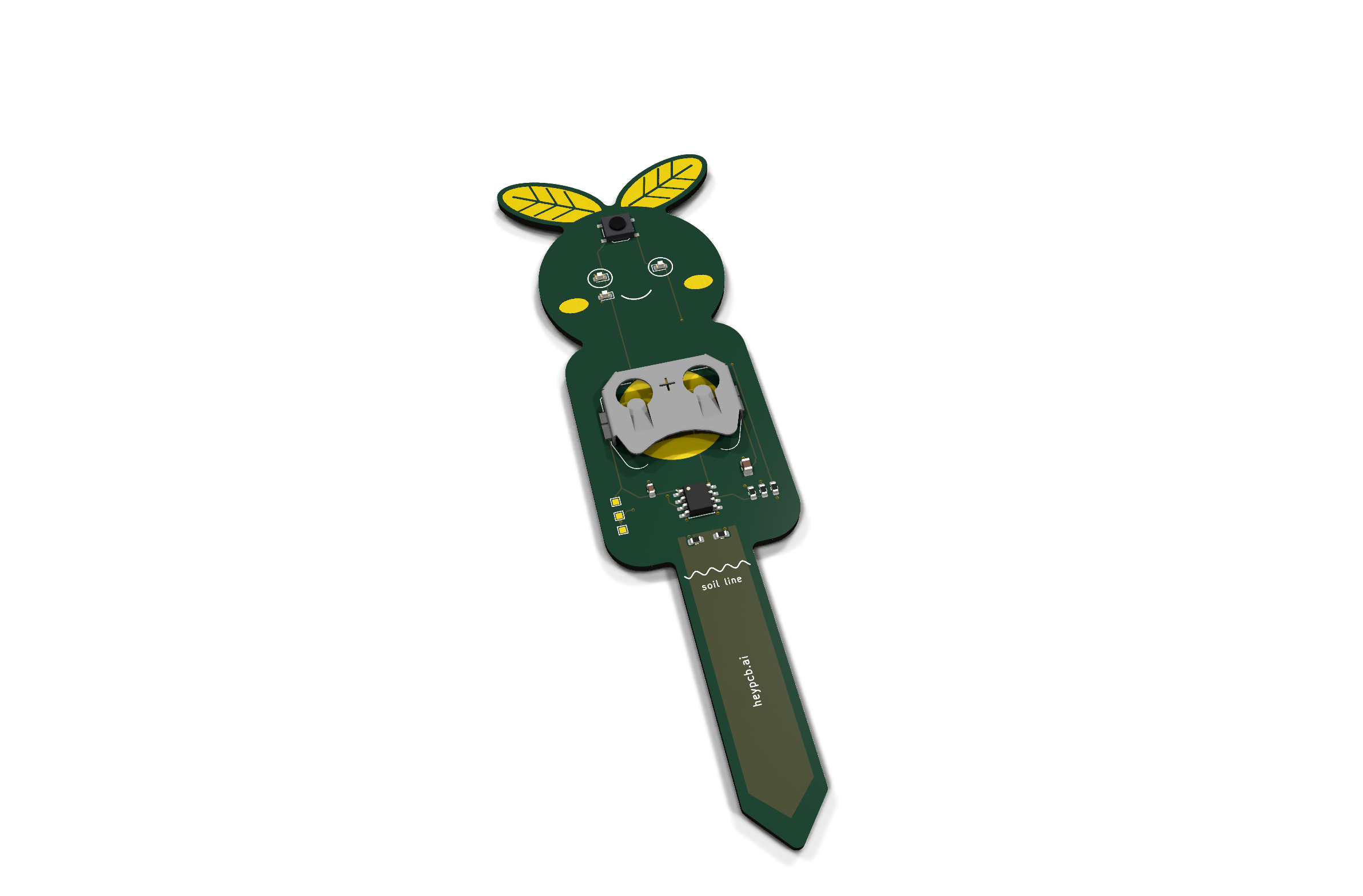
Sprout is a capacitive soil-moisture stake that lives in a plant pot on one CR2032. Its stem carries a mask-covered electrode; an ATtiny412 times how long that electrode takes to charge through 1 MΩ, and wet soil takes several times longer than dry. When the soil dries out, a blue LED tear drips under its left eye; when the plant is fine it winks. Boop the bud between its gold leaves for an instant answer.
| Layers | Size | Parts | Nets | Connections routed | Vias | ERC errors | DRC errors / unconnected / parity | BOM @100 |
|---|---|---|---|---|---|---|---|---|
| 2 | 40.4 x 128.0 mm | 13 (+3 pads) | 12 | 26 -> 0 open | 22 | 0 | 0 / 0 / 0 | $1.15 |
Not fabricated, assembled or powered yet. Every number on this page is measured by KiCad 10.0.6 on
the files in this repository (report.json, measured.json) or read
from the live JLC/LCSC catalogue (bom_cost.json).
| Spec, power budget, BOM | SPEC.md |
| Store copy | STORE_COPY.md |
| KiCad 10 project | kicad/ |
| Gerbers, drill, BOM, CPL, STEP, schematic PDF | fab/ |
| Firmware | firmware/ |
| Renders | front, back, hero, Circuit World thumbnail |
| Brief and generator | design/ |
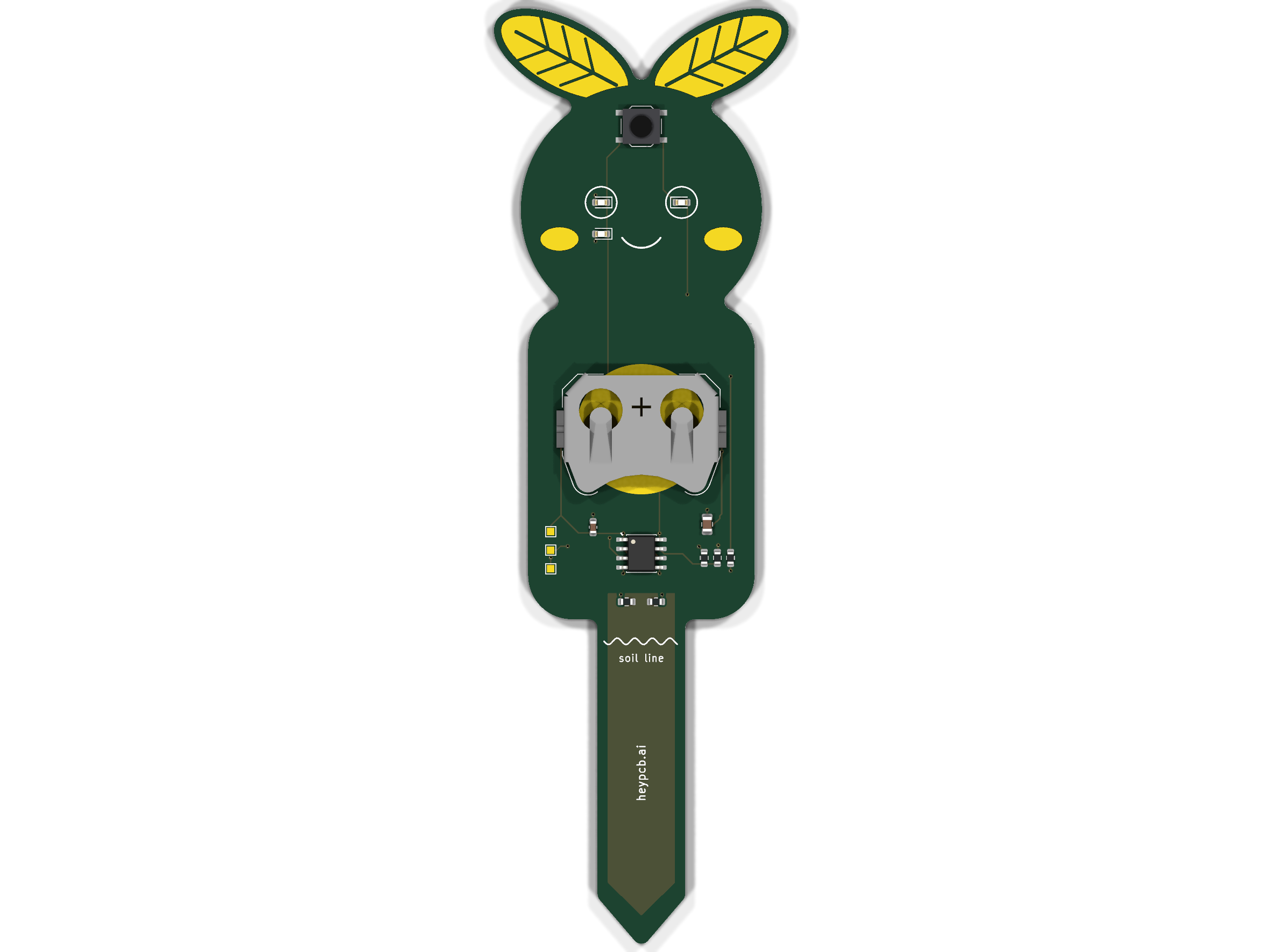
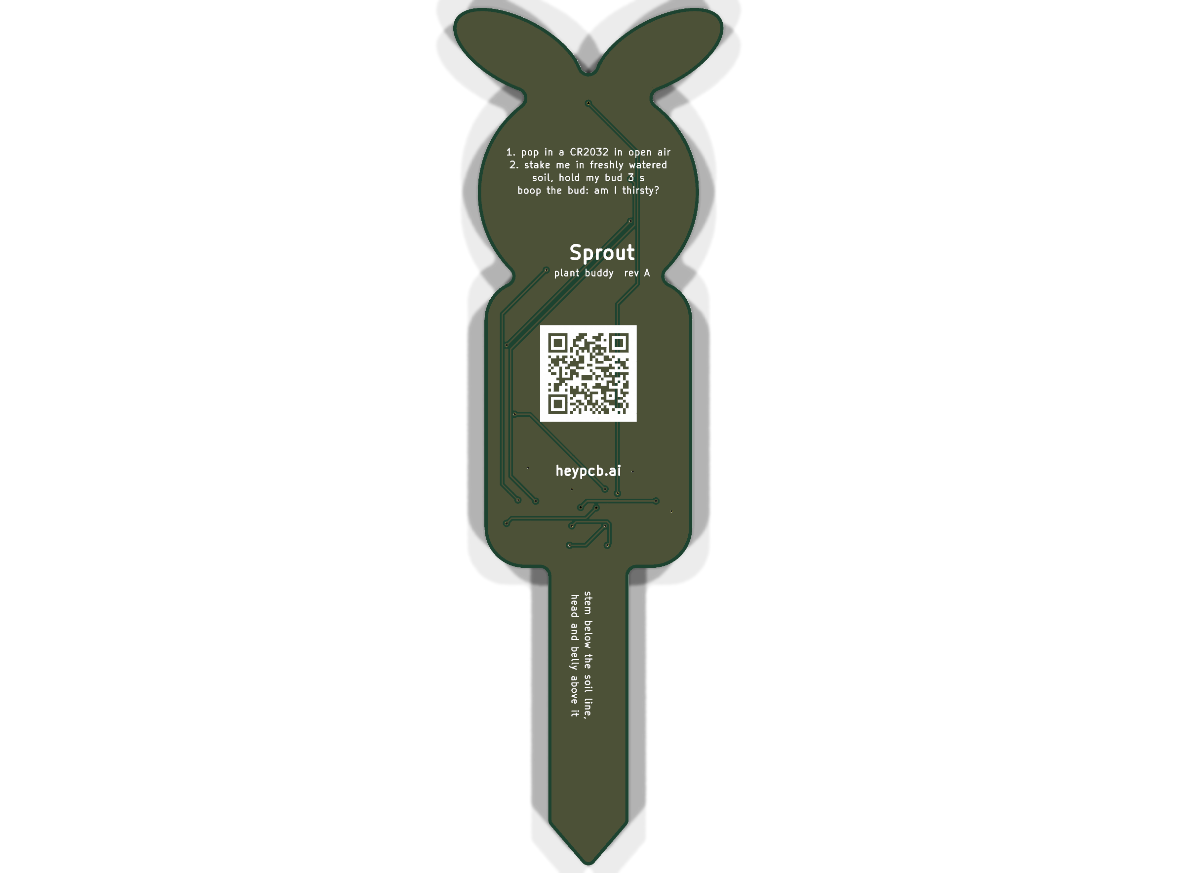
Green solder mask, White silkscreen, ENIG copper finish, 1.6 mm FR4, top-side SMT assembly. The gold art is bare copper under a mask opening (ENIG), drawn with its own keep-out so no track runs under it. The QR code on the back opens https://heypcb.ai/world/b/cdb211161e60.
Designed with the HeyPCB method on KiCad 10.0.6, headless, by the heypcb-kicad pipeline: a written
brief composed from reusable circuit blocks, every pin from KiCad's own symbol library, every part bound
to an LCSC number from a dated catalogue read, then ERC, a netlist round trip, locked placement,
Freerouting 2.4.1, pours, silkscreen and board art, DRC with schematic parity, DFM and a fab gate,
each stage gated by a measurement. design/make_brief.py regenerates the brief (outline, part
locks and art) from code.
Part of the heypcb.ai merch collection.
Hardware: CERN-OHL-S v2. Firmware: MIT (see firmware/LICENSE). KiCad's symbol, footprint and 3D
libraries used in the design are CC-BY-SA 4.0 with the KiCad library exception.
| Qty | Value | Footprint | References |
|---|---|---|---|
| 3 | 100 | Resistor_SMD:R_0603_1608Metric | R3, R4, R5 |
| 2 | Green | LED_SMD:LED_0603_1608Metric | D1, D2 |
| 1 | 100nF | Capacitor_SMD:C_0603_1608Metric | C2 |
| 1 | 10uF | Capacitor_SMD:C_0805_2012Metric | C1 |
| 1 | 1M | Resistor_SMD:R_0603_1608Metric | R1 |
| 1 | 1k | Resistor_SMD:R_0603_1608Metric | R2 |
| 1 | ATtiny412 | Package_SO:SOIC-8_3.9x4.9mm_P1.27mm | U1 |
| 1 | Blue | LED_SMD:LED_0603_1608Metric | D3 |
| 1 | CR2032 | Battery:BatteryHolder_Keystone_3034_1x20mm | BT1 |
| 1 | GND | TestPoint:TestPoint_Pad_1.0x1.0mm | TP3 |
| 1 | TS-1187A | Button_Switch_SMD:SW_Push_1P1T_XKB_TS-1187A | SW1 |
| 1 | UPDI | TestPoint:TestPoint_Pad_1.0x1.0mm | TP2 |
| 1 | VCC | TestPoint:TestPoint_Pad_1.0x1.0mm | TP1 |
HeyPCB/badge-blob
Blob, the social battery badge: The name badge that tells people whether to come say hi. KiCad 10, heypcb.ai merch.

HeyPCB/fridge-owl
Hoot, the fridge reminder owl: The fridge owl that blinks at you until you've taken your meds and had your water. KiCad 10, heypcb.ai merch.

HeyPCB/torch-cat
Torch Cat: Boop the cat's nose and its eyes light up your keyhole. KiCad 10, heypcb.ai merch.

HeyPCB/esp32-sensors-2
ESP32-S3 boards, one sensor each: KiCad 10, JLCPCB-ready, CERN-OHL-S-2.0

HeyPCB/whisker
Drop-in controller for Petoi's Nybble robot cat running the stock OpenCat firmware: ATmega328P, PCA9685, MPU-6050, USB-C, 3 A buck, protected battery input. 4-layer KiCad 10 board plus printed cradle.

superfansizhe-beep/tscircuit-stm32f302-board
STM32F302R8T6 考核板 —— 用 tscircuit 以 TypeScript 描述原理图与 PCB,9 页分页、4 层板、含完整交付物

aahmad-p/iot_tap_sensing
This repository contains an unorganized but complete copy of the code for an IoT Tap Sensing System.

HeyPCB/cable-bunny
Cable Bunny: Is it a charge-only cable? Ask the bunny. KiCad 10, heypcb.ai merch.
It measures 40.3 × 127.9 mm and has 2 copper layers, 1.6 mm thick.
16 parts, built around the ATTINY412-SSN, CC0603KRX7R9BB104, CL21A106KAYNNNE and NCD0603B1. The full list of its parts is on this page, with links to each part's symbol and footprint where PCBKit's library has them.
From the HeyPCB/plant-buddy repository on GitHub, at the commit this page was made from: the board is kicad/plant_buddy.kicad_pcb and its schematic kicad/plant_buddy.kicad_sch. PCBKit opens the board in the browser, with nothing to install.
Its repository publishes it under the CERN-OHL-S-2.0 licence: you may reuse it on that licence's terms (keep the author's notice, and for a copyleft licence share your changes alike).