
4 layers100 × 100 mm
Deneme2
Gokasimov/STM32-FOC-Control
A completely from-scratch, bare-metal implementation of Field-Oriented Control (FOC) tailored for ultra-low inductance (3 µH) drone motors (e.g., A2212).
118 parts2MIT

 Hawk453/VI_Converter_MOSFET
PCB of VI Converter with MOSFET
VI Converter MOSFET is an open-source printed circuit board by Hawk453, from the Hawk453/VI_Converter_MOSFET repository on GitHub, published under the GPL-3.0 licence. It is a 2-layer board of 76 × 53 mm with 10 parts on 8 nets, routed with 33 tracks and 3 vias.
It is built around the TLV9062ID. Its parts include 4 resistors, 3 connectors, 1 capacitor, 1 IC and 1 transistor.
PCB of VI Converter with MOSFET
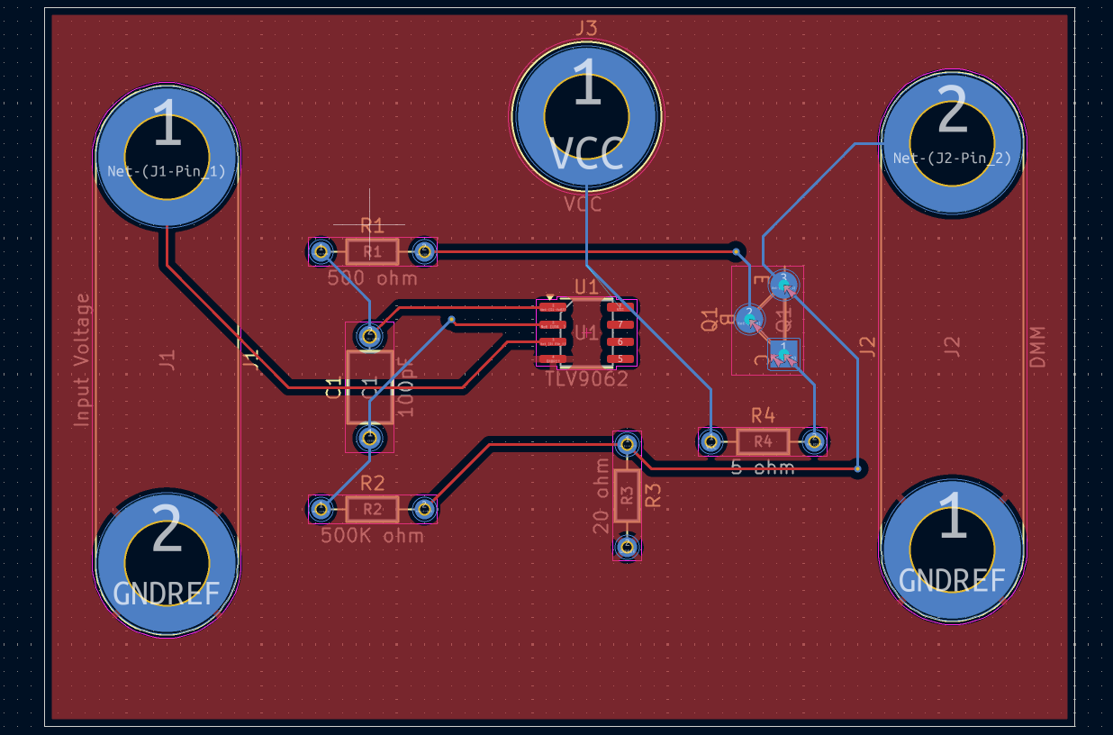
| Qty | Value | Footprint | References |
|---|---|---|---|
| 1 | 100pF | Capacitor_THT:C_Axial_L5.1mm_D3.1mm_P7.50mm_Horizontal | C1 |
| 1 | 20 ohm | Resistor_THT:R_Axial_DIN0204_L3.6mm_D1.6mm_P7.62mm_Horizontal | R3 |
| 1 | 5 ohm | Resistor_THT:R_Axial_DIN0204_L3.6mm_D1.6mm_P7.62mm_Horizontal | R4 |
| 1 | 500 ohm | Resistor_THT:R_Axial_DIN0204_L3.6mm_D1.6mm_P7.62mm_Horizontal | R1 |
| 1 | 500K ohm | Resistor_THT:R_Axial_DIN0204_L3.6mm_D1.6mm_P7.62mm_Horizontal | R2 |
| 1 | DMM | Connector:Banana_Jack_2Pin | J2 |
| 1 | Input Voltage | Connector:Banana_Jack_2Pin | J1 |
| 1 | NMOS - PMV45EN2 | PCM_Package_TO_SOT_THT_AKL_OneLayer:Transistor_Universal_CBE | Q1 |
| 1 | TLV9062 | Package_SO:SOIC-8_3.9x4.9mm_P1.27mm | U1 |
| 1 | VCC | Connector:Banana_Jack_1Pin | J3 |
Gokasimov/STM32-FOC-Control
A completely from-scratch, bare-metal implementation of Field-Oriented Control (FOC) tailored for ultra-low inductance (3 µH) drone motors (e.g., A2212).


embedded-pro/e-foc-hardware
hardware to be used with https://github.com/embedded-pro/e-foc

MLeggiero/taxelscan
TaxelScan reads a 16 × 32 pressure surface (512 taxels) at 80 frames per second by default and has been measured at 200 fps.


wemaxon/es8390-breakout
ES8390 Breakout Board with Class-D Amplifier, Line-Out/Headphone and Line-In
It measures 76 × 53 mm and has 2 copper layers, 1.6 mm thick.
10 parts, built around the TLV9062ID. The full list of its parts is on this page, with links to each part's symbol and footprint where PCBKit's library has them.
From the Hawk453/VI_Converter_MOSFET repository on GitHub, at the commit this page was made from: the board is VI_Converter_MOSFET.kicad_pcb and its schematic VI_Converter_MOSFET.kicad_sch. PCBKit opens the board in the browser, with nothing to install.
Its repository publishes it under the GPL-3.0 licence: you may reuse it on that licence's terms (keep the author's notice, and for a copyleft licence share your changes alike).