2 layers83.5 × 65.5 mm
Proyecto board
Alexanderabad/Alexander_Abad-Microcontroladores-C1-2025
Tareas de Micro C1-2025
30 parts

 H3wastooshort/usbc2dell
USB-C PD to Dell Barrel-Jack adapter
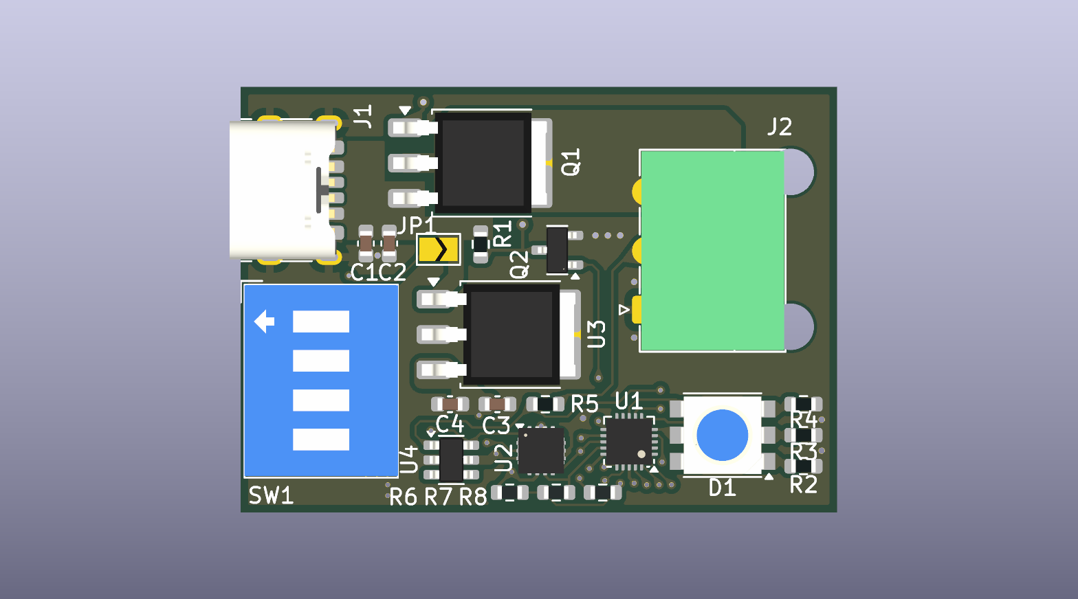
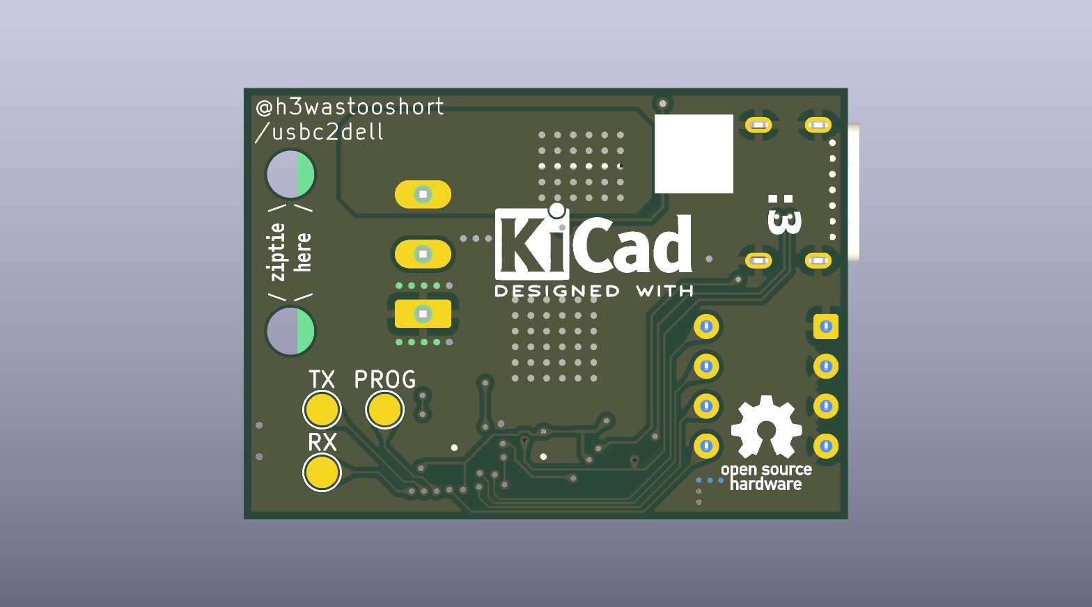
Usbc2dell is an open-source printed circuit board by H3wastooshort, from the H3wastooshort/usbc2dell repository on GitHub, published under the GPL-3.0 licence. It is a 2-layer board of 38.5 × 27.5 mm with 30 parts on 31 nets, routed with 283 tracks and 126 vias.
It is built around the ATTINY1616-MN, FUSB302BMPX and L78M05ABDT-TR, with the SRV05-4, DOD50P06 and DSWB04LHGET among its other parts. Its parts include 8 resistors, 4 capacitors, 4 ICs, 2 transistors and 2 connectors. It belongs with the AVR (ATmega, ATtiny) boards of this library.


An adapter to allow charging Laptops equipped with legacy connectors via USB Type-C.
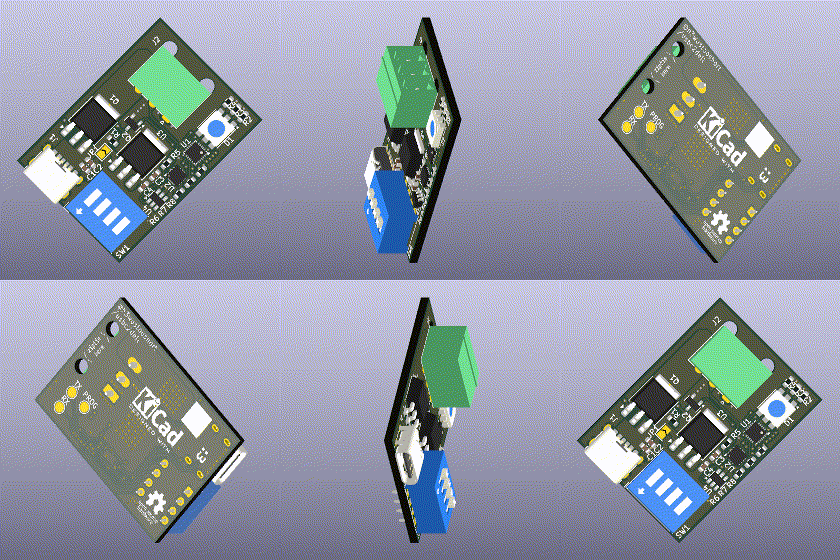
I could just slap together a USB-C PD trigger-board and a cut-off end of a cable and call it a day, but that would cause two problems:
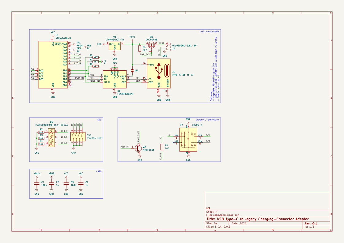
This project remidies this, by negotiating USB PD and then emulating an ID chip with the same parameters as read from the USB-C power supply. Using a 45W USB-C power supply, the laptop will know that it's only capable of 45W.
| Qty | Value | Footprint | References |
|---|---|---|---|
| 7 | 4k7 | Resistor_SMD:R_0603_1608Metric | R1, R2, R3, R4, R6, R7, R8 |
| 2 | 100n | Capacitor_SMD:C_0603_1608Metric | C1, C3 |
| 2 | 1u | Capacitor_SMD:C_0603_1608Metric | C2, C4 |
| 2 | MountingHole_3mm | MountingHole:MountingHole_3mm | HOLE1, HOLE2 |
| 1 | 100 | Resistor_SMD:R_0603_1608Metric | R5 |
| 1 | ATtiny1616-M | Package_DFN_QFN:VQFN-20-1EP_3x3mm_P0.4mm_EP1.7x1.7mm | U1 |
| 1 | DOD50P06 | Package_TO_SOT_SMD:TO-252-3_TabPin2 | Q1 |
| 1 | DSWB04LHGET | Button_Switch_THT:SW_DIP_SPSTx04_Slide_9.78x12.34mm_W7.62mm_P2.54mm | SW1 |
| 1 | FUSB302BMPX | Package_DFN_QFN:WQFN-14-1EP_2.5x2.5mm_P0.5mm_EP1.45x1.45mm | U2 |
| 1 | KiCad-Logo2_5mm_SilkScreen | Symbol:KiCad-Logo2_5mm_SilkScreen | ICON2 |
| 1 | L78M05ABDT-TR | Package_TO_SOT_SMD:TO-252-3_TabPin2 | U3 |
| 1 | MMBT5551 | Package_TO_SOT_SMD:SOT-23 | Q2 |
| 1 | OSHW-Logo_5.7x6mm_SilkScreen | Symbol:OSHW-Logo_5.7x6mm_SilkScreen | ICON1 |
| 1 | PROG | TestPoint:TestPoint_Pad_D2.0mm | TP1 |
| 1 | RX | TestPoint:TestPoint_Pad_D2.0mm | TP3 |
| 1 | SRV05-4 | Package_TO_SOT_SMD:SOT-23-6 | U4 |
| 1 | SolderJumper_2_Open | Jumper:SolderJumper-2_P1.3mm_Open_TrianglePad1.0x1.5mm | JP1 |
| 1 | TC5050RGBF08-3CJH-AF53A | LED_SMD:LED_RGB_5050-6 | D1 |
| 1 | TX | TestPoint:TestPoint_Pad_D2.0mm | TP2 |
| 1 | TYPE-C-31-M-17 | Connector_USB:USB_C_Receptacle_HRO_TYPE-C-31-M-17 | J1 |
| 1 | WJ15EDGRC-3.81-3P | Connector_Phoenix_MC:PhoenixContact_MC_1,5_3-G-3.81_1x03_P3.81mm_Horizontal | J2 |
Alexanderabad/Alexander_Abad-Microcontroladores-C1-2025
Tareas de Micro C1-2025

SK-Electronics-Consulting/electronics-widgets
Small, Custom Tools for Electronics

niektb/sluisbrinkie-eurorack-published
Published Modules of the Sluisbrinkie project

jibrilsharafi/EnergyMe-Home
Smart energy meter capable of monitoring up to 16 channels. Supports MQTT, REST API, Modbus TCP, InfluxDB, AWS IoT Core. Friendly UI and fully open source (PCB, schematics, components, source code)

tobycm/nRF52840-with-nPM1300-devboard
just a simple devboard for the nRF52840 equipped with lots of 2.4Ghz technologies and the nPM1300 PMIC for power management, both ICs are made by Nordic semiconductor

snarrn/Raspberry_Pi_Pico_MultiBoard
This is a PCB with OLED, LaserTag, two Radio Receivers, Oscillotor, Sound Card for PC, Smoke Detector, LEDs, Maze Game, Accelerometer, Motor/Speaker Drivers, two Proximity Detecters, Thermometer, Photo Detector, Etc.


It measures 38.5 × 27.5 mm and has 2 copper layers, 1.6 mm thick.
30 parts, built around the ATTINY1616-MN, FUSB302BMPX, L78M05ABDT-TR and SRV05-4. The full list of its parts is on this page, with links to each part's symbol and footprint where PCBKit's library has them.
From the H3wastooshort/usbc2dell repository on GitHub, at the commit this page was made from: the board is hardware/usbc2dell.kicad_pcb and its schematic hardware/usbc2dell.kicad_sch. PCBKit opens the board in the browser, with nothing to install.
Its repository publishes it under the GPL-3.0 licence: you may reuse it on that licence's terms (keep the author's notice, and for a copyleft licence share your changes alike).