
2 layers69.6 × 33.5 mm

 Gallan99/smart_glove
A compact smart-glove project for measuring finger bending with five piezoresistive strain sensors. The system combines a custom constant-current analog front end, Arduino data acquisition and a simple Python interface…
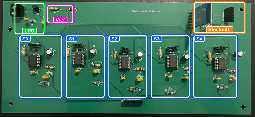
Test1 is an open-source printed circuit board by Gallan99, from the Gallan99/smart_glove repository on GitHub. It is a 2-layer board of 215.3 × 96.5 mm with 60 parts on 40 nets, routed with 333 tracks and 30 vias.
It is built around the CA3140. Its parts include 22 capacitors, 14 resistors, 9 connectors, 6 ICs and 5 diodes.
A compact smart-glove project for measuring finger bending with five piezoresistive strain sensors. The system combines a custom constant-current analog front end, Arduino data acquisition and a simple Python interface for viewing and saving measurements.
| File | Description |
|---|---|
stable_current_5sensors.ino | Arduino firmware for reading and filtering five strain sensors. |
gui_script_v2.py | Tkinter interface for serial measurements, live plotting and data logging. |
kicad/ | KiCad project containing the schematic and PCB layout of the five-channel board. |
images/ | Photos of the prototype and representative sensor measurements. |
The custom board contains five independent sensor-readout channels, a voltage reference, voltage regulation and Bluetooth connectivity.
Open kicad/test1.kicad_pro in KiCad to inspect the complete schematic and PCB design.
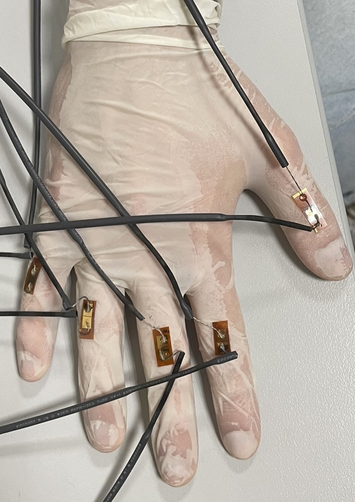
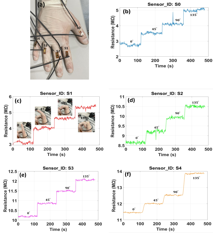
The sensors produce a clear resistance change as the fingers bend from 0° to 135°.
Open stable_current_5sensors.ino in the Arduino IDE.
Check the calibration constants RSET_OHMS, VNODE_VOLTS and ADC_REF_VOLTS for the specific board.
Upload the firmware to the Arduino and open the serial connection at 115200 baud.
Install the Python dependencies:
pip install pyserial matplotlibStart the desktop interface:
python gui_script_v2.pyNote: The Python interface is included in its original single-channel logging form. The Arduino file outputs five sensor channels, so the serial-field selection in the Python parser must be adapted when using the two files together.
The complete smart-glove system is described in the following preprint:
| Qty | Value | Footprint | References |
|---|---|---|---|
| 7 | 1kΩ | Resistor_THT:R_Axial_DIN0207_L6.3mm_D2.5mm_P7.62mm_Horizontal | R2, R3, R6, R8, R10, R12, R13 |
| 6 | 330kΩ | Resistor_THT:R_Axial_DIN0207_L6.3mm_D2.5mm_P7.62mm_Horizontal | R4, R5, R7, R9, R11, R14 |
| 5 | 100nF | Capacitor_THT:C_Disc_D5.0mm_W2.5mm_P2.50mm | C4, C9, C13, C17, C21 |
| 5 | 10nF | Capacitor_THT:C_Disc_D5.0mm_W2.5mm_P2.50mm | C6, C10, C14, C18, C22 |
| 5 | 10uF | Capacitor_THT:CP_Radial_D5.0mm_P2.00mm | C5, C8, C12, C16, C20 |
| 5 | 47pF | Capacitor_THT:C_Disc_D5.0mm_W2.5mm_P2.50mm | C3, C7, C11, C15, C19 |
| 5 | CA3140 | Package_DIP:DIP-8_W7.62mm_LongPads | U1, U3, U4, U5, U6 |
| 5 | Conn_01x02_Pin | Connector_PinSocket_2.54mm:PinSocket_1x02_P2.54mm_Vertical | J2, J4, J5, J6, J7 |
| 5 | D_Zener | Diode_THT:D_DO-35_SOD27_P7.62mm_Horizontal | D1, D2, D3, D4, D5 |
| 4 | , , , | ||
| 1 | 0.1uF | Capacitor_THT:C_Disc_D5.0mm_W2.5mm_P2.50mm | C2 |
| 1 | 0.33uF | Capacitor_THT:C_Disc_D5.0mm_W2.5mm_P2.50mm | C1 |
| 1 | 47kΩ | Resistor_THT:R_Axial_DIN0207_L6.3mm_D2.5mm_P7.62mm_Horizontal | R1 |
| 1 | Conn_01x03 | Connector_PinSocket_2.54mm:PinSocket_1x03_P2.54mm_Vertical | J9 |
| 1 | Conn_01x06 | Connector_PinSocket_2.54mm:PinSocket_1x06_P2.54mm_Vertical | J3 |
| 1 | Conn_01x06_Pin | Connector_PinSocket_2.54mm:PinSocket_1x06_P2.54mm_Vertical | J8 |
| 1 | L78L05_TO92 | Package_TO_SOT_THT:TO-92_Inline | U2 |
| 1 | Screw_Terminal_01x02 | TerminalBlock_Phoenix:TerminalBlock_Phoenix_MKDS-1,5-2-5.08_1x02_P5.08mm_Horizontal | J1 |


electrickery/MicroKit09MK2
A recreation of an MC6809 Single Board Computer from the 1980's

gabrielebarola/Energy-Meter-progetto-PCTO
Progetto per il percorso di PCTO 2021/2022

PhyPiDAQ/EducatorsGuide
Tutorial for educators and examples of educational physics experiments

alexmrqt/Philips-GAM-48-303-daughterboard
A daughterboard to fix Philips GAM 48-303 soldering stations with faulty U106BS chips.

benishor/w7zoi-sa-ad8307-log-amp
Kicad files for the new AD8307 log amp for W7ZOI spectrum analyzer.

Bonya0/SPRO2-Group-8
Github repository for Electornics Semester Project 2 Group 8
It measures 215.3 × 96.5 mm and has 2 copper layers, 1.61 mm thick.
60 parts, built around the CA3140. The full list of its parts is on this page, with links to each part's symbol and footprint where PCBKit's library has them.
From the Gallan99/smart_glove repository on GitHub, at the commit this page was made from: the board is kicad/test1.kicad_pcb and its schematic kicad/test1.kicad_sch. PCBKit opens the board in the browser, with nothing to install.
Its repository states no licence, so its author keeps all rights: ask Gallan99 before reusing the design.