

2 layers63.5 × 33 mm
 BadenLab/nTCscope2
Repository for nTC
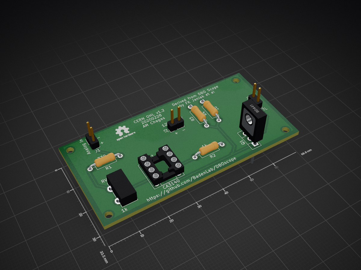
Etl driver pcb is an open-source printed circuit board by BadenLab, from the BadenLab/nTCscope repository on GitHub, published under the MIT licence. It is a 2-layer board of 69.6 × 33.5 mm with 15 parts on 12 nets, routed with 29 tracks and 0 vias.
It is built around the CA3140 and BD441. Its parts include 4 resistors, 3 connectors, 1 IC and 1 transistor.

This project is licensed under the [GNU General Public License v3.0]
Non-Telecentric 2P two-photon microscopy for 3D random access mesoscale imaging
FK Janiak, P Bartel, R Bale, T Yoshimatsu, E Komulainen, M Zhou, K Staras, LL Prieto-Godino, T Euler, M Maravall, T Baden
| Qty | Value | Footprint | References |
|---|---|---|---|
| 2 | 10 | Resistor_THT:R_Axial_DIN0207_L6.3mm_D2.5mm_P10.16mm_Horizontal | R3, R4 |
| 1 | 12V power | Connector_PinHeader_2.54mm:PinHeader_1x02_P2.54mm_Vertical | J2 |
| 1 | 1k | Resistor_THT:R_Axial_DIN0207_L6.3mm_D2.5mm_P10.16mm_Horizontal | R2 |
| 1 | 1k | Potentiometer_THT:Potentiometer_ACP_CA9-H3,8_Horizontal | RV1 |
| 1 | 330 | Resistor_THT:R_Axial_DIN0207_L6.3mm_D2.5mm_P10.16mm_Horizontal | R1 |
| 1 | Analog in | Connector_PinHeader_2.54mm:PinHeader_1x02_P2.54mm_Vertical | J1 |
| 1 | BD441 | Package_TO_SOT_THT:TO-126-3_Vertical | Q1 |
| 1 | CA3140 | Package_DIP:DIP-8_W7.62mm_Socket | U1 |
| 1 | to_ETL | Connector_PinHeader_2.54mm:PinHeader_1x02_P2.54mm_Vertical | J3 |
The 10 most common of 15 parts.


electrickery/MicroKit09MK2
A recreation of an MC6809 Single Board Computer from the 1980's

gabrielebarola/Energy-Meter-progetto-PCTO
Progetto per il percorso di PCTO 2021/2022

PhyPiDAQ/EducatorsGuide
Tutorial for educators and examples of educational physics experiments

alexmrqt/Philips-GAM-48-303-daughterboard
A daughterboard to fix Philips GAM 48-303 soldering stations with faulty U106BS chips.

benishor/w7zoi-sa-ad8307-log-amp
Kicad files for the new AD8307 log amp for W7ZOI spectrum analyzer.

Bonya0/SPRO2-Group-8
Github repository for Electornics Semester Project 2 Group 8

Gallan99/smart_glove
A compact smart-glove project for measuring finger bending with five piezoresistive strain sensors. The system combines a custom constant-current analog front end, Arduino data acquisition and a simple Python interface…
It measures 69.6 × 33.5 mm and has 2 copper layers, 1.6 mm thick.
15 parts, built around the CA3140 and BD441. The full list of its parts is on this page, with links to each part's symbol and footprint where PCBKit's library has them.
From the BadenLab/nTCscope repository on GitHub, at the commit this page was made from: the board is ETL/etl_driver_pcb/etl_driver_pcb.kicad_pcb. PCBKit opens the board in the browser, with nothing to install.
Its repository publishes it under the MIT licence: you may reuse it on that licence's terms (keep the author's notice, and for a copyleft licence share your changes alike).