2 layers78 × 60 mm

 DLehenbauer/faux-pi-zero4
RP2040 dev board in a Raspberry Pi Zero compatible form factor. Includes DVI and SD Card.
Faux pi-0 is an open-source printed circuit board by DLehenbauer, from the DLehenbauer/faux-pi-zero repository on GitHub. It is a 4-layer board of 65 × 30 mm with 63 parts on 78 nets, routed with 1,243 tracks and 111 vias.
It is built around the RP2040, W25Q128JVSIQ and AMS1117-3.3. Its parts include 22 resistors, 17 capacitors, 7 connectors, 3 ICs and 2 diodes. It belongs with the microcontroller boards and interfaces and adapters boards and the RP2040 boards of this library.


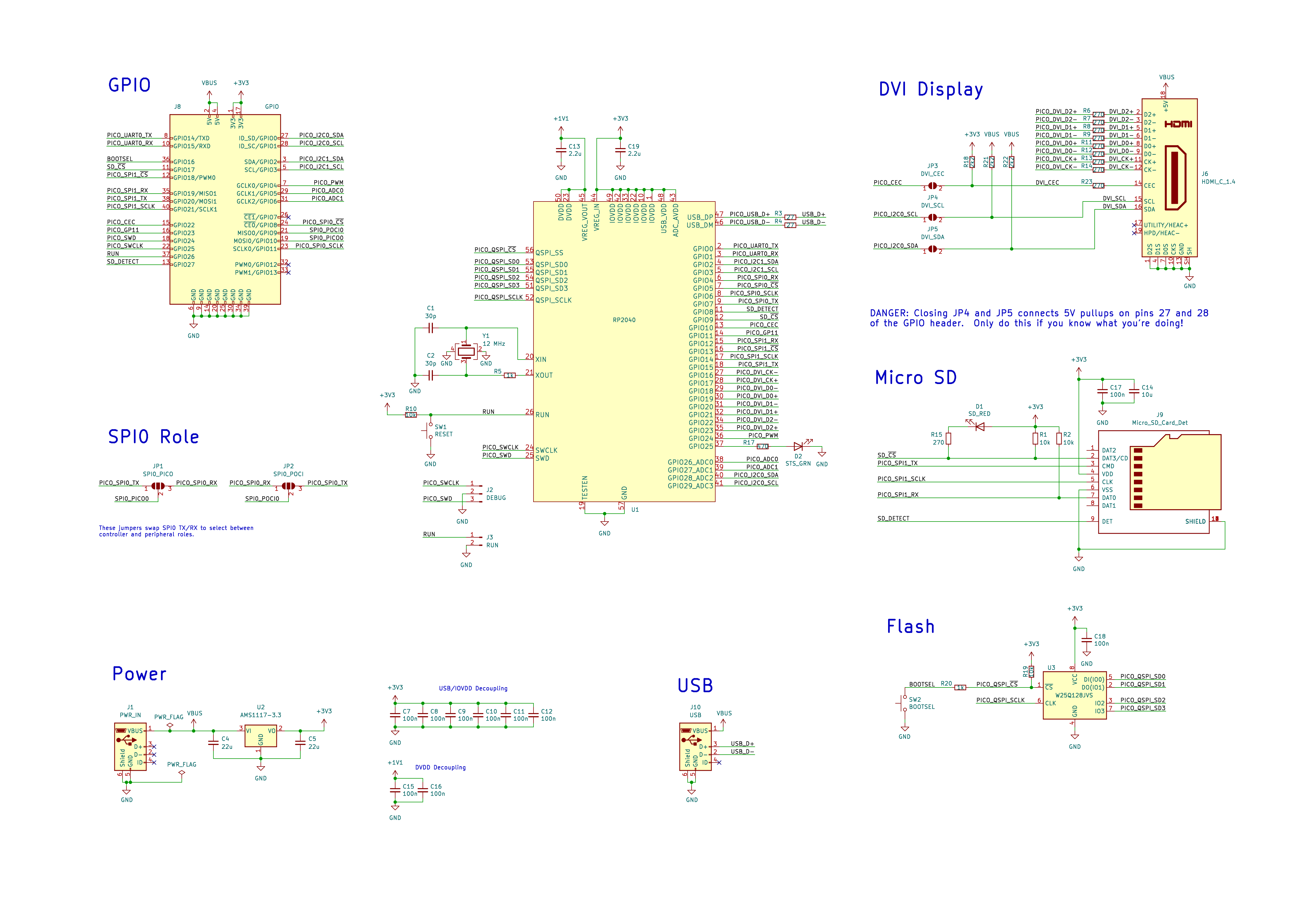
Open hardware RP2040 dev board in a Raspberry Pi Zero compatible form factor. Includes Mini HDMI (via bitbanged DVI) and microSD.

This board aids with migrating a project from the Pi Zero to the RP2040 while retaining the option of moving back to the Pi Zero in the future. It has the same footprint as the Pi Zero and a partially compatible pinout, making it convenient to support both the RP2040 and Pi Zero in the same design.
Works, but 1 of 2 boards received by JLCPCB had a solder bridge on the RP2040. Looking at JLCPCB's EasyEDA footprints, it looks like JLCPCB used longer pads for the RP2040. I'd recommend using a custom footprint and extending the pads, which hopefully will avoid defects.
A couple other things I'd change in retrospect:
DVI and microSD both appear to work with a basic test. I've exercised DVI, USB (host), SPI1, and the debug header quite a bit (all good). Other functionality is either lightly tested or untested.
See schematic for more details.

| Pi Pin | Pico Pin | Pi GPIO | Pico GP | Function | Notes |
|---|---|---|---|---|---|
| 1, 17 | 36 | 3V3 (Out) | |||
| 2, 4 | 39 | VSYS | |||
| 2, 4 | 40 | VBUS | |||
| 3 | 4 | GPIO 02 | GP 02 | I2C_SDA | |
| 5 | 5 | GPIO 03 | GP 03 | I2C_SCL | |
| 6, 9, 14, 20, 25, 30, 34, 39 | 3, 8, 13, 18, 23, 28, 33, 38, DBG-2 | GND | |||
| 7 | GPIO 04 | GP 24 | |||
| 8 | 1 | GPIO 14 | GP 00 | UART0 TX | |
| 10 | 2 | GPIO 15 | GP 01 | UART0 RX | |
| 11 | 12 | GPIO 17 | GP 09 | SD_CSn | Can be used as GP with SD card removed. Note 10k pullup. |
| 12 | 17 | GPIO 18 | GP 13 | SPI1_CSn | Can be used to share SPI1 with SD card. |
| 13 | 11 | GPIO 27 | GP 08 | SD_DET | Can be used as GP with SD card removed. |
| 15 | 14 | GPIO 22 | GP 10 | DVI_CEC | DVI_CEC when JP3 closed. See schematic. |
| 16 | 15 | GPIO 23 | GP 11 | ||
| 18 | DBG-3 | GPIO 24 | SWD | ||
| 19 | 6/10 | GPIO 10 | GP 04/07 | SPI0_RX/TX | Select controller or peripheral via JP1 and JP2. See schematic. |
| 21 | 10/6 | GPIO 09 | GP 07/04 | SPI0_TX/RX | Select controller or peripheral via JP1 and JP2. See schematic. |
| 22 | DBG-1 | GPIO 25 | SWCLK | ||
| 23 | 9 | GPIO 11 | GP 06 | SPI0_SCLK | |
| 24 | 7 | GPIO 08 | GP 05 | SPI0_CSn | |
| 26 | GPIO 07 | ||||
| 27 | 34 | GPIO 00 | GP 28 | I2C_SCL | DVI_SDA when JP4 closed. See schematic. |
| 28 | GPIO 01 | GP 29 | |||
| 29 | 31 | GPIO 05 | GP 26 | ||
| 31 | 32 | GPIO 06 | GP 27 | I2C_SDA | DVI_SDA when JP5 closed. See schematic. |
| 32 | GPIO 12 | ||||
| 33 | GPIO 13 | ||||
| 35 | 16 | GPIO 19 | GP 12 | SPI1_RX / SD_DAT | Can be used as GP with SD card removed. Note 10k pullup. |
| 36 | GPIO 16 | BOOTSEL | |||
| 37 | 30 | GPIO 26 | RUN | ||
| 38 | 20 | GPIO 20 | GP 15 | SPI1_TX / SD_CMD | Can be used as GP with SD card removed. |
| 40 | 19 | GPIO 21 | GP 14 | SPI1_SCLK / SD_CLK | Can be used as GP with SD card removed. |
| GP 23 | DVI_D2+ | ||||
| 21 | GP 16 | DVI_CK- | |||
| 22 | GP 17 | DVI_CK+ | |||
| 24 | GP 18 | DVI_D0- | |||
| 25 | GP 19 | DVI_D0+ | |||
| 26 | GP 20 | DVI_D1- | |||
| 27 | GP 21 | DVI_D1+ | |||
| 29 | GP 22 | DVI_D2- | |||
| 35 | N/C | ||||
| 37 | 3V3_EN | ||||
| LED | GP 25 |
(Click image to view PDF)
| Qty | Value | Footprint | References |
|---|---|---|---|
| 10 | 100n | Capacitor_SMD:C_0402_1005Metric | C7, C8, C9, C10, C11, C12, C15, C16, C17, C18 |
| 10 | 270 | Resistor_SMD:R_0603_1608Metric | R6, R7, R8, R9, R11, R12, R13, R14, R15, R23 |
| 4 | 10k | Resistor_SMD:R_0402_1005Metric | R1, R2, R10, R19 |
| 4 | MountingHole_2.7mm_M2.5 | MountingHole:MountingHole_2.7mm_M2.5 | MH1, MH2, MH3, MH4 |
| 3 | 2k2 | Resistor_SMD:R_0402_1005Metric | R18, R21, R22 |
| 2 | 1k | Resistor_SMD:R_0402_1005Metric | R5, R20 |
| 2 | 2.2u | Capacitor_SMD:C_0402_1005Metric | C13, C19 |
| 2 | 22u | Capacitor_SMD:C_0805_2012Metric | C4, C5 |
| 2 | 27 | Resistor_SMD:R_0603_1608Metric | R3, R4 |
| 2 | 30p | Capacitor_SMD:C_0402_1005Metric | C1, C2 |
| 1 | 10u | Capacitor_SMD:C_0402_1005Metric | C14 |
| 1 | 12 MHz | Crystal:Crystal_SMD_3225-4Pin_3.2x2.5mm | Y1 |
| 1 | 470 | Resistor_SMD:R_0402_1005Metric | R17 |
| 1 | AMS1117-3.3 | Package_TO_SOT_SMD:SOT-223-3_TabPin2 | U2 |
| 1 | BOOTSEL | Button_Switch_THT:SW_PUSH_6mm | SW2 |
| 1 | DEBUG | Connector_PinHeader_2.54mm:PinHeader_1x03_P2.54mm_Vertical | J2 |
| 1 | DVI_CEC | Jumper:SolderJumper-2_P1.3mm_Open_RoundedPad1.0x1.5mm | JP3 |
| 1 | DVI_SCL | Jumper:SolderJumper-2_P1.3mm_Open_RoundedPad1.0x1.5mm | JP4 |
| 1 | DVI_SDA | Jumper:SolderJumper-2_P1.3mm_Open_RoundedPad1.0x1.5mm | JP5 |
| 1 | GPIO | Connector_PinHeader_2.54mm:PinHeader_2x20_P2.54mm_Vertical | J8 |
| 1 | HDMI_C_1.4 | JLCPCB:HDMI-SMD_HDMI-201 | J6 |
| 1 | Micro_SD_Card_Det | JLCPCB:SIM-SMD_8P-1040310811 | J9 |
| 1 | PWR_IN | JLCPCB:MICRO-USB_MICRO-USB-17 | J1 |
| 1 | RESET | Button_Switch_THT:SW_PUSH_6mm | SW1 |
| 1 | RP2040 | Package_DFN_QFN:QFN-56-1EP_7x7mm_P0.4mm_EP3.2x3.2mm_ThermalVias | U1 |
| 1 | RUN | Connector_PinHeader_2.54mm:PinHeader_1x02_P2.54mm_Vertical | J3 |
| 1 | SD_RED | LED_SMD:LED_0603_1608Metric | D1 |
| 1 | SPI0_PICO | Jumper:SolderJumper-3_P1.3mm_Open_RoundedPad1.0x1.5mm | JP1 |
| 1 | SPI0_POCI | Jumper:SolderJumper-3_P1.3mm_Open_RoundedPad1.0x1.5mm | JP2 |
| 1 | STS_GRN | LED_SMD:LED_0603_1608Metric | D2 |
| 1 | USB | JLCPCB:MICRO-USB_MICRO-USB-17 | J10 |
| 1 | W25Q128JVS | Package_SO:SOIC-8_5.23x5.23mm_P1.27mm | U3 |

OpenJBOD/rp2040
This repository contains the hardware design files OpenJBOD RP2040 Baseboard.

jpconstantineau/PyKey60
The PyKey60 is a custom programmable mechanical keyboard with a standard ANSI 60% keyboard layout compatible with any cases made for the GH60. The PyKey60 uses mechanical switches (Cherry MX type).

victorhook/asac-fc
asac fc is an rp2040 based flight controller made for FPV drone flying


MReavley/CyberSliceKeyboard
42/36 key ergo split keyboard using a RP2040


autonomous-ai/autonomous-circuit
Chat with AI, get a verified PCB and a fab packet you can order.
It measures 65 × 30 mm and has 4 copper layers, 1.65 mm thick.
63 parts, built around the RP2040, W25Q128JVSIQ and AMS1117-3.3. The full list of its parts is on this page, with links to each part's symbol and footprint where PCBKit's library has them.
From the DLehenbauer/faux-pi-zero repository on GitHub, at the commit this page was made from: the board is hw/faux-pi-0.kicad_pcb and its schematic hw/faux-pi-0.kicad_sch. PCBKit opens the board in the browser, with nothing to install.
Its repository states no licence, so its author keeps all rights: ask DLehenbauer before reusing the design.