
4 layers38.5 × 47 mm

 CDonohoe-Designs/EdgeLink_S3_Cellular
EdgeLink S3 Cellular is a four-layer embedded hardware platform combining an ESP32-S3 controller, SIM7080G cellular/GNSS modem, USB-C, battery power management and environmental/motion sensing.
EdgeLink S3 Cellular is an open-source printed circuit board by CDonohoe-Designs, from the CDonohoe-Designs/EdgeLink_S3_Cellular repository on GitHub. It is a 4-layer board of 56 × 52 mm with 114 parts on 148 nets, routed with 785 tracks and 289 vias.
It is built around the ESP32-S3-MINI-1-N8, SIM7080G and BMP384, with the SHT40-AD1B-R2, TPS63802DLAR and BMI323 among its other parts. Its parts include 30 capacitors, 30 resistors, 11 ICs, 8 diodes and 3 switches. It belongs with the ESP32 boards of this library.


ESP32-S3 Embedded Hardware Design | LTE-M / NB-IoT | GNSS | Battery Power Management | Four-Layer PCB | KiCad
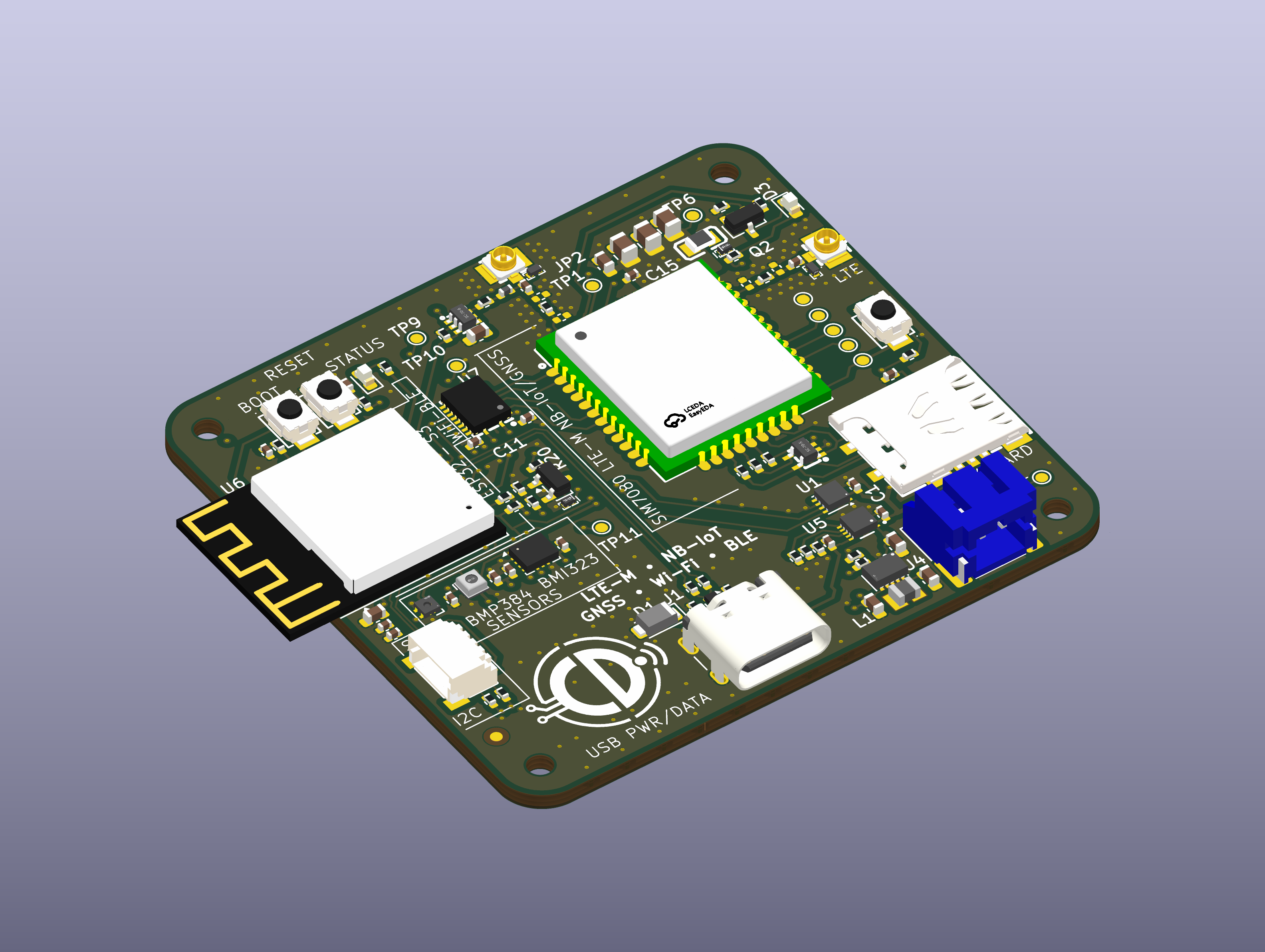
EdgeLink S3 Cellular is a four-layer embedded hardware platform combining an ESP32-S3 controller, SIM7080G cellular/GNSS modem, USB-C, battery power management and environmental/motion sensing.
I developed the Rev A schematic and PCB as an engineering portfolio project, demonstrating system architecture, wireless module integration, power-tree design, digital interfaces, multilayer layout and manufacturing documentation.
Project status: The schematic, PCB and manufacturing package are complete as design deliverables. Rev A is an unbuilt design; hardware bring-up and physical performance testing have not been completed.
| Resource | Contents |
|---|---|
| Illustrated engineering portfolio (PDF) | Six-page visual case study with genuine PCB renders, schematic extracts and manufacturing evidence |
| Editable portfolio (Word) | Editable report |
| Portfolio images | PCB top/bottom views, four copper layers, circuit extracts and CAD renders |
| System architecture | Functional system diagram |
| Complete schematic PDF | Hierarchical schematic |
| Editable KiCad project | PCB, schematic and supporting libraries |
| Manufacturing package | Gerbers, BOM and component placement |
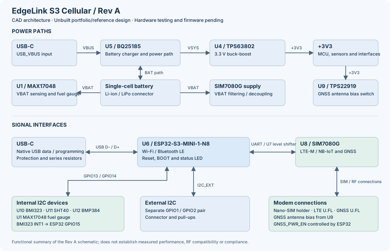
| Subsystem | Implementation |
|---|---|
| Controller | ESP32-S3-MINI-1-N8 with Wi-Fi/Bluetooth LE and native USB |
| Cellular and positioning | SIMCom SIM7080G LTE-M / NB-IoT and GNSS |
| Charging and power path | TI BQ25185 |
| 3.3 V regulation | TI TPS63802 buck-boost |
| Battery monitoring | MAX17048 fuel gauge |
| Motion sensing | Bosch BMI323 six-axis IMU |
| Environmental sensing | SHT40 temperature/humidity and BMP384 pressure |
| External interfaces | USB-C, Nano-SIM, LTE/GNSS U.FL, battery and I²C |
USB-C provides input power and native USB data. The BQ25185 manages the battery and system supply, while the TPS63802 generates the main 3.3 V rail. The cellular modem is powered from the battery supply through its input filtering. The sensor subsystem uses I²C connections to the ESP32-S3.
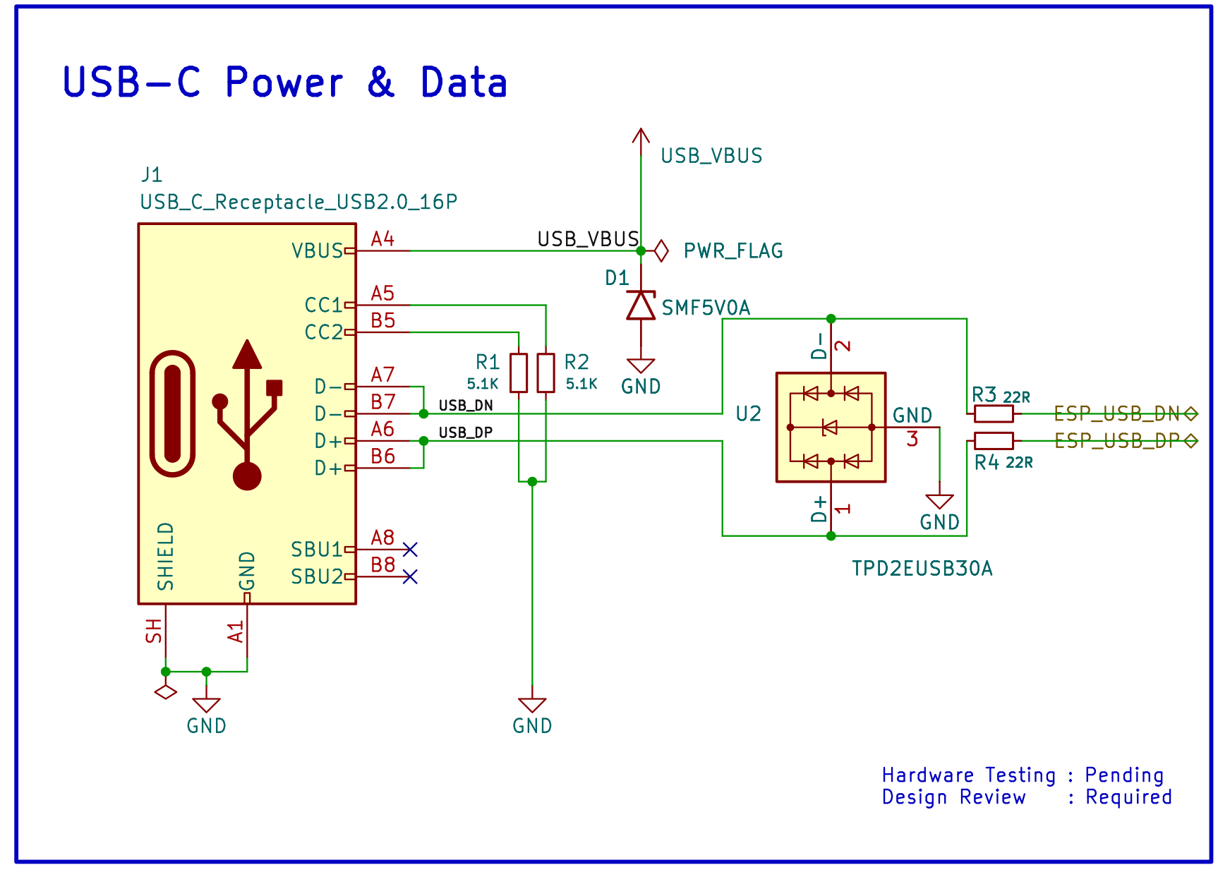
The hierarchical schematic separates power and USB, ESP32-S3 processing, cellular/GNSS and sensor interfaces. Key circuits include battery charging and regulation, modem power and UART connectivity, RF antenna interfaces, USB-C protection and digital sensor integration.
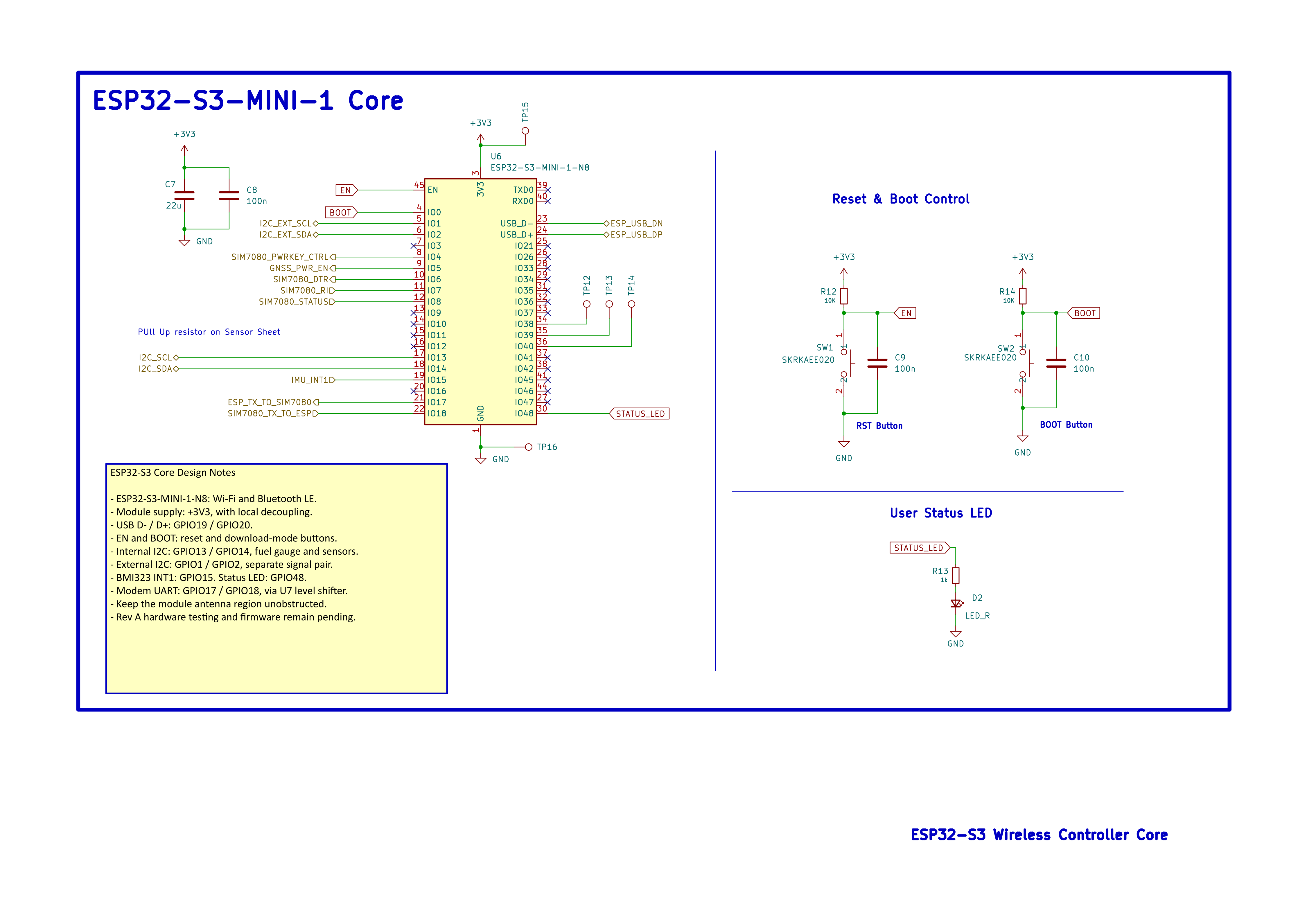
The ESP32-S3-MINI-1-N8 schematic brings together the controller supply and decoupling, native USB connections, modem control signals, I²C interfaces, reset/boot circuitry and status LED.
The Rev A PCB integrates power conversion, digital processing, wireless communications and sensors on a nominal 56 × 52 mm board. The layout uses four copper layers with local component decoupling and functional grouping of power, RF and digital circuitry.
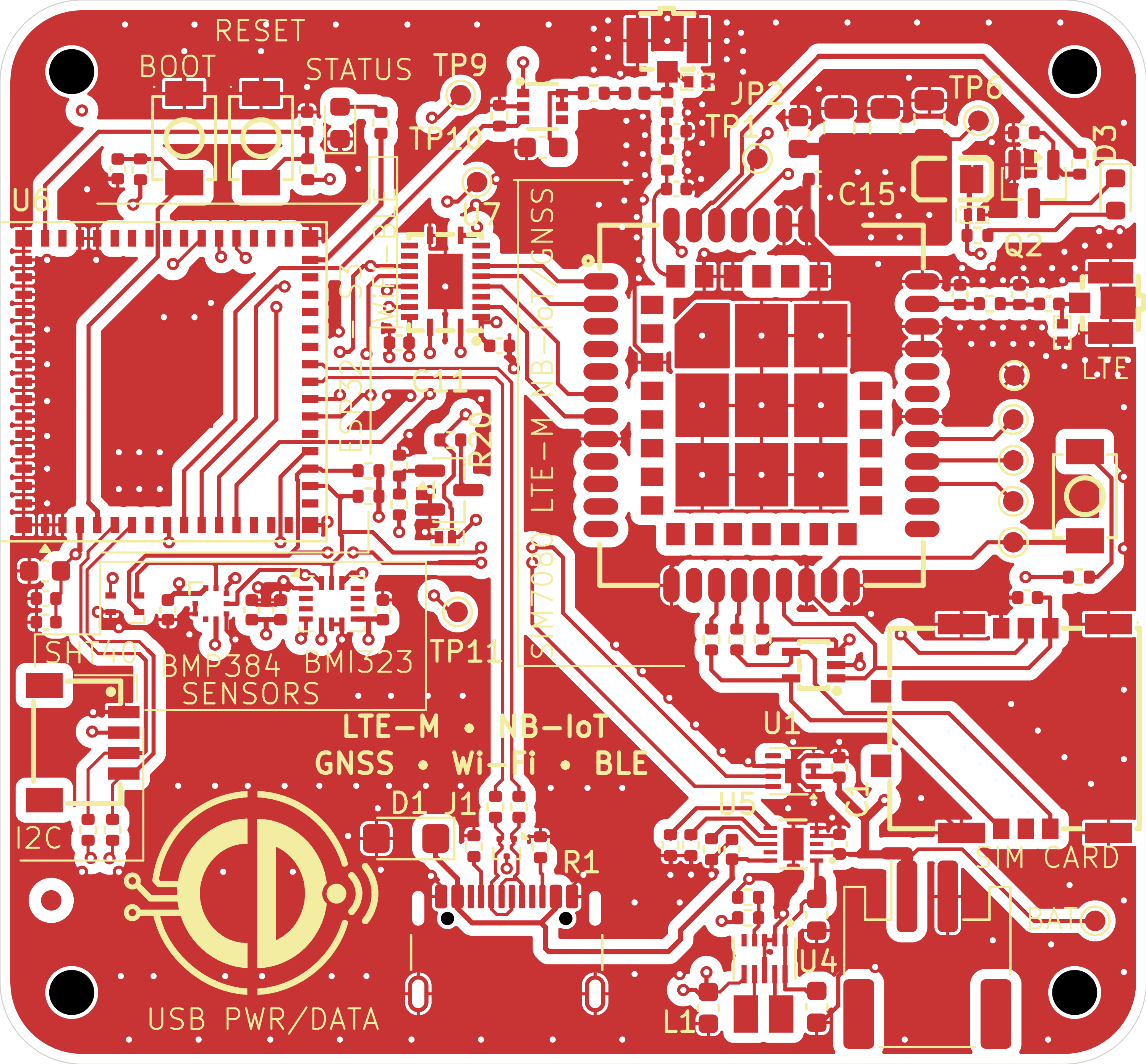
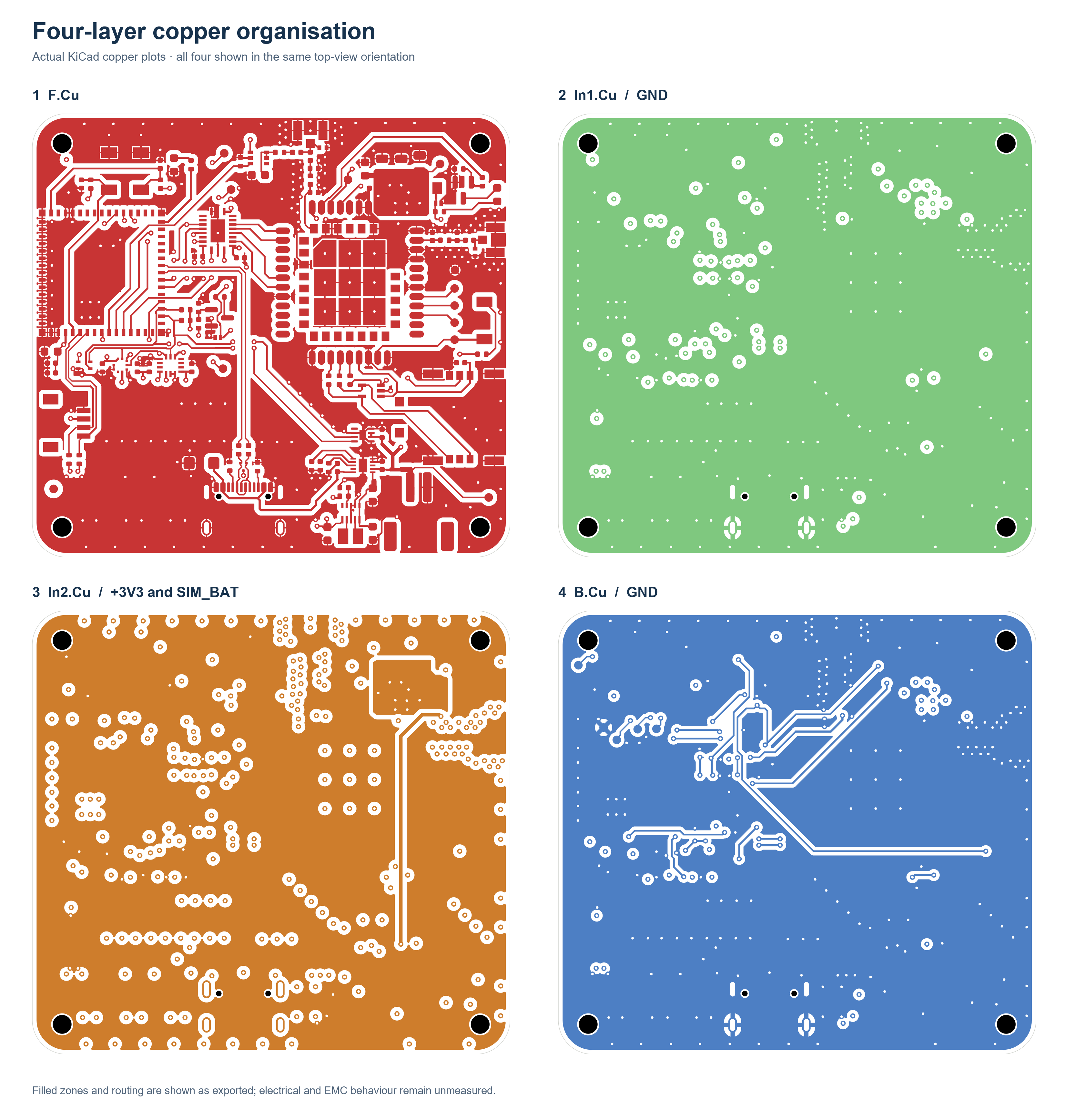
Additional PCB views and genuine KiCad CAD renders are included in the illustrated portfolio.
The Rev A package includes fabrication Gerbers, drill files, a supplier-oriented BOM with LCSC references and component placement data for JLCPCB-oriented assembly preparation.
The assembly BOM contains 46 component groups covering 89 fitted references, matched by the component placement list.
| Location | Contents |
|---|---|
| Portfolio | Illustrated PDF, Word report and supporting images |
| KiCad source | Editable design and local assets |
| Architecture notes | Functional interfaces and power tree |
| Manufacturing | Fabrication and assembly files |
| Verification records | Detailed internal design-check documentation |
| References | Manufacturer sources and CAD attribution |
Tools: KiCad 10, ESP32-S3 hardware design, wireless module integration, LCSC/JLCPCB-oriented manufacturing workflow and Git/GitHub.
No project-wide licence has been selected. Third-party assets retain their respective rights; see references.
| Qty | Value | Footprint | References |
|---|---|---|---|
| 12 | 100n | Capacitor_SMD:C_0402_1005Metric | C1, C8, C9, C10, C11, C12, C13, C26, C27, C28, C29, C30 |
| 6 | 4.7k | Resistor_SMD:R_0402_1005Metric | R15, R16, R30, R31, R32, R33 |
| 6 | PWRKEY | TestPoint:TestPoint_Pad_D1.0mm | TP11, TP12, TP13, TP14, TP15, TP16 |
| 5 | 22R | Resistor_SMD:R_0402_1005Metric | R3, R4, R22, R23, R24 |
| 4 | 1k | Resistor_SMD:R_0402_1005Metric | R6, R13, R19, R20 |
| 4 | DNP | Capacitor_SMD:C_0402_1005Metric | C19, C20, C21, C22 |
| 3 | 100u | Capacitor_SMD:C_0805_2012Metric | C16, C17, C18 |
| 3 | 10K | Resistor_SMD:R_0402_1005Metric | R12, R14, R25 |
| 3 | 1u | Capacitor_SMD:C_0402_1005Metric | C3, C4, C15 |
| 3 | SKRKAEE020 | SKRKAEE020:SW-SMD_L3.9-W3.0-P4.45 | SW1, SW2, SW3 |
| 2 | 0R | Resistor_SMD:R_0402_1005Metric | R27, R28 |
| 2 | 100n | Capacitor_SMD:C_0603_1608Metric | C14, C25 |
| 2 | 100p | Capacitor_SMD:C_0402_1005Metric | C23, C24 |
| 2 | 10u | Capacitor_SMD:C_0603_1608Metric | C2, C5 |
| 2 | 22u | Capacitor_SMD:C_0603_1608Metric | C6, C7 |
| 2 | 47k | Resistor_SMD:R_0402_1005Metric | R17, R18 |
| 2 | 5.1K | Resistor_SMD:R_0402_1005Metric | R1, R2 |
| 2 | LED_R | LED_SMD:LED_0603_1608Metric | D2, D3 |
| 2 | LXES15AAA1-153_C7472903 | LXES15AAA1-153:DFN1006-2L-BI | D7, D8 |
| 2 | MMBT3904 | Package_TO_SOT_SMD:SOT-23 | Q1, Q2 |
| 2 | U.FL-R-SMT-1 | U:RF-SMD_FRF05002-JSS103M | JP1, JP2 |
| 1 | 0.47u | DFE201612E-R47M_P2:INDC2016X120N | L1 |
| 1 | 100k | Resistor_SMD:R_0402_1005Metric | R26 |
| 1 | 1042240820 | 1042240820:SIM-SMD_1042240820 | Card1 |
| 1 | 10R | Resistor_SMD:R_0402_1005Metric | R29 |
| 1 | 10k | Resistor_SMD:R_0402_1005Metric | R8 |
| 1 | 18k | Resistor_SMD:R_0402_1005Metric | R7 |
| 1 | 47n | Inductor_SMD:L_0402_1005Metric | L3 |
| 1 | 511k | Resistor_SMD:R_0402_1005Metric | R9 |
| 1 | 91k | Resistor_SMD:R_0402_1005Metric | R10 |
| 1 | BLM21PG221SN1D | BLM21PG221SN1D:L0805 | L2 |
| 1 | BMI323 | Package_LGA:Bosch_LGA-14_3x2.5mm_P0.5mm | U10 |
| 1 | BMP384 | Sensor_Footprints:BMP390_LGA10_2x2mm | U12 |
| 1 | BQ25185 | BQ25185:WSON10_DLH_TEX | U5 |
| 1 | ESD5651N-2/TR | ESD5651N-2:DFN1006-2L-BI-1 | D6 |
| 1 | ESDA6V1W5 | ESDA6V1W5:SC-70-5_L2.1-W1.3-P0.65-LS2.1-BR | D4 |
| 1 | ESP32-S3-MINI-1-N8 | RF_Module:ESP32-S2-MINI-1 | U6 |
| 1 | ESP_TX_TO_SIM7080 | TestPoint:TestPoint_Pad_D1.0mm | TP9 |
| 1 | GND | TestPoint:TestPoint_Pad_D1.0mm | TP7 |
| 1 | LiPo 1S | Connector_JST:JST_PH_S2B-PH-SM4-TB_1x02-1MP_P2.00mm_Horizontal | JBT1 |
| 1 | MAX17048G+T10 | Package_DFN_QFN:TDFN-8-1EP_2x2mm_P0.5mm_EP0.8x1.2mm | U1 |
| 1 | SHT40-AD1B-R2 | Sensor_Footprints:SHT4x_DFN4_1.5x1.5mm | U11 |
| 1 | SIM7080G | SIM7080G:LCC-SMD_SIM7080G | U8 |
| 1 | SIM7080_TX_TO_ESP | TestPoint:TestPoint_Pad_D1.0mm | TP10 |
| 1 | SIM_BAT | TestPoint:TestPoint_Pad_D1.0mm | TP6 |
| 1 | SIM_USB_DM | TestPoint:TestPoint_Pad_D1.0mm | TP4 |
| 1 | SIM_USB_DP | TestPoint:TestPoint_Pad_D1.0mm | TP3 |
| 1 | SIM_USB_VBUS | TestPoint:TestPoint_Pad_D1.0mm | TP5 |
| 1 | SM04B-SRSS-TB | SM04B-SRSS-TB:CONN-SMD_4P-P1.00_SM04B-SRSS-TB-LF-SN | CN1 |
| 1 | SMF5V0A | Diode_SMD:D_SMF | D1 |
| 1 | TPD2EUSB30A | Package_TO_SOT_SMD:Texas_DRT-3 | U2 |
| 1 | TPRCLAMP01892PWQC | TPRCLAMP01892PWQC:DFN1006-2L-BI-1 | D5 |
| 1 | TPS22919DCKR | TPS22919DCKR:SC-70-6_L2.2-W1.3-P0.65-LS2.1-BR | U9 |
| 1 | TPS63802DLAR | TPS63802:TPS63802DLAR | U4 |
| 1 | TXB0108RGYR | TXB0108RGYR:VQFN-20_L4.5-W3.5-P0.50-BL-EP | U7 |
| 1 | USB_BOOT | TestPoint:TestPoint_Pad_D1.0mm | TP2 |
| 1 | USB_C_Receptacle_USB2.0_16P | Connector_USB:USB_C_Receptacle_GCT_USB4105-xx-A_16P_TopMnt_Horizontal | J1 |
| 1 | VBAT | TestPoint:TestPoint_Pad_D1.0mm | TP8 |
| 1 | VDD_EXT | TestPoint:TestPoint_Pad_D1.0mm | TP1 |
The 109 most common of 114 parts.

Open-Air-Foundation/pcb-module-ce-card
The CE card adds 4G cellular connectivity (LTE Cat 1) to AirGradient monitors. It can be used in the AirGradient Open Air, the AirGradient ONE, and the Open Air Max.


lucasnoce/IC-LevelSensor_v2
Water level sensor with NBIoT data transmission

jekhor/bluetooth-traffic-mon
Researching of traffic monitoring by Bluetooth scanning

williamjroche/Drone_Flight_Controller
This is a GPS-Denied Autonomous Drone that uses computer vision to fly with radio transmission override. Autonomy is a work in progress.

It measures 56 × 52 mm and has 4 copper layers, 1.56 mm thick.
114 parts, built around the ESP32-S3-MINI-1-N8, SIM7080G, BMP384 and SHT40-AD1B-R2. The full list of its parts is on this page, with links to each part's symbol and footprint where PCBKit's library has them.
From the CDonohoe-Designs/EdgeLink_S3_Cellular repository on GitHub, at the commit this page was made from: the board is hardware/kicad/EdgeLink_S3_Cellular_RevA/EdgeLink_S3_Cellular.kicad_pcb and its schematic hardware/kicad/EdgeLink_S3_Cellular_RevA/00_System_Block_Diagram.kicad_sch. PCBKit opens the board in the browser, with nothing to install.
Its repository states no licence, so its author keeps all rights: ask CDonohoe-Designs before reusing the design.