4 layers
MTQ Driver
BrownSpaceEngineering/PVDX-ADCS-PMB
Avionics files related to ADCS and Perovskite schematics, pcb design, and documentation
4 parts1

 BrownSpaceEngineering/PVDX-ADCS-PMB1
Avionics files related to ADCS and Perovskite schematics, pcb design, and documentation
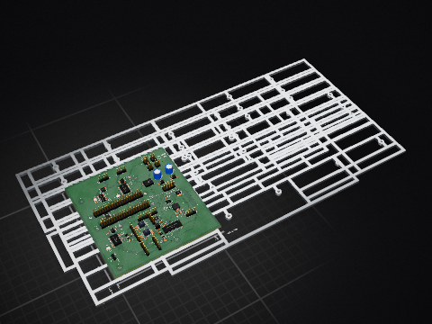
PVDX ADCS PMB is an open-source printed circuit board by BrownSpaceEngineering, from the BrownSpaceEngineering/PVDX-ADCS-PMB repository on GitHub. It is a 4-layer board of 82.5 × 82.5 mm with 114 parts on 112 nets, routed with 1,351 tracks and 185 vias.
It is built around the INA226AIDGSR, TLV9001IDCKR-MS and ADG734BRUZ, with the MCP23017-E/SO among its other parts. Its parts include 39 capacitors, 37 resistors, 19 ICs and 7 connectors.


Combined ADCS actuation and Perovskite Measurement Board. Drives magnetorquers for attitude control and performs IV-sweep measurement of the perovskite solar cell payload.
This board serves two subsystems on one physical PCB:
Board sheets:
PVDX-ADCS-PMB/
├── PVDX-ADCS-PMB.kicad_pro / .kicad_sch / .kicad_pcb / .step
├── fp-lib-table, sym-lib-table, design-block-lib-table
├── schematics/          # sub-sheets
│   ├── connectors.kicad_sch
│   ├── magnetorquers.kicad_sch
│   ├── perovskites.kicad_sch
│   └── photodiodes.kicad_sch
├── libs/
│   ├── footprints.pretty/
│   ├── symbols/
│   ├── 3dmodels/
│   └── Library.kicad_blocks/
│       └── MTQ_Driver.kicad_block/   # deprecated
└── manufacturing/
    └── rev-<N>_<date>/
        ├── gerbers/
        ├── bom/
└── plots/0b0100000, INA226 at 0b1000000 (address-pin strapped) — confirm no collisions with other devices sharing this board's I2C bus before finalizing layout.MTQ_Driver Design Block is reused at the schematic level only; PCB-side placement is manual (Swap command), not trusted to Design Block replication.| Rev | Date | Notes | Location |
|---|---|---|---|
| 1.1 | 9/4/26 | Prepared for fabrication | manufacturing/rev-1.0_2026-05-15/ |
| Qty | Value | Footprint | References |
|---|---|---|---|
| 18 | 150p | Capacitor_SMD:C_0603_1608Metric | C45, C46, C47, C48, C49, C50, C51, C52, C53, C54, C55, C56, C57, C58, C59, C60 +2 |
| 18 | 2k2 | Resistor_SMD:R_0603_1608Metric | R40, R41, R42, R43, R44, R45, R46, R47, R48, R49, R50, R51, R52, R53, R54, R55 +2 |
| 16 | 100R | Resistor_SMD:R_0603_1608Metric | R3, R4, R5, R6, R7, R8, R9, R10, R11, R12, R13, R14, R15, R16, R17, R18 |
| 11 | 100n | Capacitor_SMD:C_0603_1608Metric | C37, C38, C39, C40, C41, C42, CBY2, CBY6, CBY7, CBY8, CBY9 |
| 10 | 100n | Capacitor_SMD:C_0402_1005Metric | C1, C2, C3, C4, C5, C6, C7, C8, C9, CBY5 |
| 9 | OPA2381AIDGKR | footprints:DGK8 | U11, U12, U13, U14, U15, U16, U17, U18, U19 |
| 4 | ADG734BRUZ | footprints:RU_20_ADI | U6, U7, U8, U9 |
| 4 | MountingHole | footprints:MountingHole_3.4mm_M3_PVDX | H1, H2, H3, H4 |
| 3 | 22u | footprints:GRM18x | CB1, CB2, CB3 |
| 3 | DRV8837CDSGR | footprints:DSG8_P9X1P6_TEX | U3, U4, U10 |
| 1 | 10R | Resistor_SMD:R_0603_1608Metric | RSH1 |
| 1 | 10k | Resistor_SMD:R_0603_1608Metric | R37 |
| 1 | 12k | Resistor_SMD:R_0603_1608Metric | R2 |
| 1 | 21k | Resistor_SMD:R_0603_1608Metric | R1 |
| 1 | Conn_01x02 | Connector_PinHeader_2.54mm:PinHeader_1x02_P2.54mm_Vertical | J4 |
| 1 | Conn_01x03 | Connector_PinHeader_2.54mm:PinHeader_1x03_P2.54mm_Vertical | J6 |
| 1 | Conn_01x06 | Connector_PinHeader_2.54mm:PinHeader_1x06_P2.54mm_Vertical | J3 |
| 1 | Conn_01x09 | Connector_PinHeader_2.54mm:PinHeader_1x09_P2.54mm_Vertical | J7 |
| 1 | Conn_01x17 | Connector_PinHeader_2.54mm:PinHeader_1x17_P2.54mm_Vertical | J5 |
| 1 | Conn_01x18 | footprints:FH34SRJ18S05SH50 | J2 |
| 1 | Conn_02x18_Row_Letter_Last | Connector_PinHeader_2.54mm:PinHeader_2x18_P2.54mm_Vertical | J1 |
| 1 | INA226AIDGSR | Package_SO:TSSOP-10_3x3mm_P0.5mm | U2 |
| 1 | LOGO | footprints:hotdog | G*** |
| 1 | LOGO | footprints:snoopy | G*** |
| 1 | LOGO | LOGO | G*** |
| 1 | MCP23017-E/SO | Package_SO:SOIC-28W_7.5x17.9mm_P1.27mm | U5 |
| 1 | NetTie_2 | NetTie:NetTie-2_SMD_Pad0.5mm | NT1 |
| 1 | TLV9001IDCKR | Package_TO_SOT_SMD:SOT-353_SC-70-5 | U1 |
BrownSpaceEngineering/PVDX-ADCS-PMB
Avionics files related to ADCS and Perovskite schematics, pcb design, and documentation

befinitiv/cmd-z5-pager
Replacement PCB & Software to turn Sony CMD-Z5 into a Meshtastic/Lorawan pager


pierrechevalier83/ferris
A low profile split keyboard designed to satisfy one single use case elegantly


techie66/EngineDataLogger-EngineData
Arduino code for SleepyPi that is attached to main datalogger. Reads engine sensors.

techie66/EngineDataLogger-FrontControls
Arduino code for front controls device.
It measures 82.5 × 82.5 mm and has 4 copper layers, 1.6 mm thick.
114 parts, built around the INA226AIDGSR, TLV9001IDCKR-MS, ADG734BRUZ and MCP23017-E/SO. The full list of its parts is on this page, with links to each part's symbol and footprint where PCBKit's library has them.
From the BrownSpaceEngineering/PVDX-ADCS-PMB repository on GitHub, at the commit this page was made from: the board is PVDX-ADCS-PMB.kicad_pcb and its schematic PVDX-ADCS-PMB.kicad_sch. PCBKit opens the board in the browser, with nothing to install.
Its repository states no licence, so its author keeps all rights: ask BrownSpaceEngineering before reusing the design.