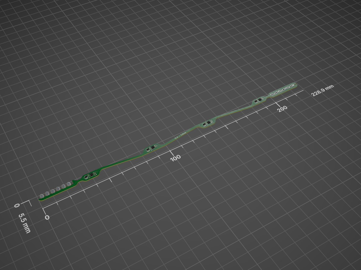
2 layers228.9 × 5.5 mm
TMP117 section 10cm
BerkeleyLab/DxP-sensor-probes
Hardware design for the DxP (Distributed sensor Profiling) sensor probe.
38 parts1
 BerkeleyLab/DxP-sensor-probes1
Hardware design for the DxP (Distributed sensor Profiling) sensor probe.
TMP117 section 5cm is an open-source printed circuit board by BerkeleyLab, from the BerkeleyLab/DxP-sensor-probes repository on GitHub. It is a 2-layer board of 228.9 × 5.5 mm with 38 parts on 22 nets, routed with 3,397 tracks and 59 vias.
It is built around the TMP117AIDRVR and SN74LVC1G175DCK. Its parts include 10 resistors, 8 capacitors and 8 ICs. It belongs with the sensors and measurement boards of this library.


This repository contains the PCB designs for DxP (Distributed sensor Profiling) sensor probes—including sensor sections and the connector/extension pieces needed to assemble probe chains.
Not included: the data logger hardware (it lives in the separate DxP data logger repository).
Not included: the mechanical probe tube/epoxy assembly instructions. This repo focuses on the PCB designs only.
The sensor probe concept is based on cascaded I²C sensor arrays using a solderless board-to-board connector to build probes of configurable length. Each probe section maintains the required sensor spacing and enables deformation (ADXL345) and/or temperature (TMP117) profiling.
Reference (sensor probes):
Wielandt et al., “Low-Power, Flexible Sensor Arrays with Solderless Board-to-Board Connectors for Monitoring Soil Deformation and Temperature” (Sensors, 2022) DOI: 10.3390/s22072814
Sensor probes in this repository connect to the DxP data logger (separate repo), which performs wireless data logging and connectivity for distributed deployments.
Reference (data logger / network):
Wielandt et al., “TDD LoRa and Delta Encoding in Low-Power Networks of Environmental Sensor Arrays for Temperature and Deformation Monitoring” (J. Signal Process. Syst., 2023) DOI: 10.1007/s11265-023-01834-2
Adjacent probe boards are connected using a mechanical + electrical snap-fit made entirely in PCB technology:
(For clarity: the extension/adapter connector combinations in this repo are engineering building blocks; the connector technology used between standard sensor sections is described in the Sensors 2022 paper and U.S. Patent US 11,582,870 B2.)
end_connector/
off-axis_end_connector/
TMP117_section_5cm/
TMP117_section_10cm/
TMP117-ADXL345_section_5cm/
These boards extend probe length without adding sensors (and support mixed rigid/flexible assembly concepts). These connector pieces and combinations were not published in literature.
extension_board_MF/
extension_board_MM/
FF_connector/
sensor_board_outline/
Each PCB design directory typically contains:
*.sch, *.kicad_pcb, plus associated project files (*.kicad_pro, *.kicad_prl)*_BOM.csv-style files where applicable (e.g., in end_connector/fab/)fab/ (per-project fabrication exports)fp-lib-table, sym-lib-table, and fp-info-cache/README.md, LICENSE.mdand users.md (self-reported user tracking)users.md: self-reported adopters/projects using the DxP probe hardware (recommended).If you want, I can also tighten this further to match the logger README format even more closely (shorter “Hardware overview” + “Repository contents” only), but the text above should already be accurate and concise for a probe-repo release.
| Qty | Value | Footprint | References |
|---|---|---|---|
| 8 | 100n | Capacitor_SMD:C_0402_1005Metric | C1, C2, C3, C4, C5, C6, C7, C8 |
| 6 | C1a | TestPoint:subsilk | TP1, TP4, TP6, TP8, TP10, TP12 |
| 6 | C1b | PCB_connector:oval_hole_1 | TP2, TP5, TP7, TP9, TP11, TP13 |
| 4 | 1k | Resistor_SMD:R_0402_1005Metric | R3, R5, R6, R7 |
| 4 | 470 | Resistor_SMD:R_0402_1005Metric | R2, R8, R9, R10 |
| 4 | SN74LVC1G175DCK | Package_TO_SOT_SMD:Texas_R-PDSO-G6 | U1, U3, U4, U5 |
| 4 | TMP117AIDRVR | Package_SON:WSON-6-1EP_2x2mm_P0.65mm_EP1x1.6mm | U2, U6, U7, U8 |
| 2 | DNP | Resistor_SMD:R_0402_1005Metric | R1, R4 |
BerkeleyLab/DxP-sensor-probes
Hardware design for the DxP (Distributed sensor Profiling) sensor probe.

BerkeleyLab/DxP-sensor-probes
Hardware design for the DxP (Distributed sensor Profiling) sensor probe.

BerkeleyLab/DxP-sensor-probes
Hardware design for the DxP (Distributed sensor Profiling) sensor probe.

BerkeleyLab/DxP-sensor-probes
Hardware design for the DxP (Distributed sensor Profiling) sensor probe.

BerkeleyLab/DxP-sensor-probes
Hardware design for the DxP (Distributed sensor Profiling) sensor probe.

BerkeleyLab/DxP-sensor-probes
Hardware design for the DxP (Distributed sensor Profiling) sensor probe.

BerkeleyLab/DxP-sensor-probes
Hardware design for the DxP (Distributed sensor Profiling) sensor probe.

BerkeleyLab/DxP-data-logger
Hardware design for the DxP (Distributed sensor Profiling) data logger that connects to a DxP sensor probe.

sparkfun/SparkFun_Soft_Power_Switch_Mk2
Documentation, example code, and hardware for the SparkFun Soft Power Switch - JST 2mm.

sparkfun/SparkFun_Soft_Power_Switch_USB-C
Documentation, example code, and hardware for the SparkFun Soft Power Switch - USB-C.

Meo98/picostack
Stackable, contract-driven module system for the Raspberry Pi Pico — open hardware, built by code


will127534/OneInchEye
A One Inch CMOS sensor (IMX283) camera board designed for Raspberry Pi


will127534/ShutterEye
A simple camera board using SC910GS 1" 4K@30fps global shutter sensor
It measures 228.9 × 5.5 mm and has 2 copper layers, 0.79 mm thick.
38 parts, built around the TMP117AIDRVR and SN74LVC1G175DCK. The full list of its parts is on this page, with links to each part's symbol and footprint where PCBKit's library has them.
From the BerkeleyLab/DxP-sensor-probes repository on GitHub, at the commit this page was made from: the board is TMP117_section_5cm/TMP117_section_5cm.kicad_pcb and its schematic FF_connector/FF_connector.kicad_sch. PCBKit opens the board in the browser, with nothing to install.
Its repository states no licence, so its author keeps all rights: ask BerkeleyLab before reusing the design.