2 layers79.2 × 59.2 mm
Diodes IncorporatedExtended
-55℃~+150℃ 1 P-Channel 1.357nF 1.3W 12V 15.8nC@4.5V 1V 235pF 31mΩ@4.5V 5.2A 504pF P-Channel SOT-23 MOSFETs ROHS
The DMP1045U is a MOSFET made by Diodes Incorporated in a SOT-23 package with 3 pins. -55℃~+150℃ 1 P-Channel 1.357nF 1.3W 12V 15.8nC@4.5V 1V 235pF 31mΩ@4.5V 5.2A 504pF P-Channel SOT-23 MOSFETs ROHS.
PCBKit's library has its KiCad symbol (Pinmap_Generic:Q_PMOS_1G_2S_3D, from PCBKit's generic symbols) and its footprint (Package_TO_SOT_SMD:SOT-23, from KiCad's library), ready for a KiCad board. 6,537 are in stock at JLCPCB (part C177033). 24 open-source boards in 20 repositories on GitHub use it.
| Parameter | Conditions | As printed | Page |
|---|---|---|---|
| Drain-Source Voltage VDSS | TA = +25°C, unless otherwise specified | max -12 V | 2 |
| Gate-Source Voltage VGSS | TA = +25°C; ±8 V | min -8 · max 8 V | 2 |
| Continuous Drain Current (Note 5) VGS = -4.5V ID | Steady State; TA = +25°C; minimum recommended pad layout, single sided | max 4 A | 2 |
| Continuous Drain Current (Note 5) VGS = -4.5V ID | Steady State; TA = +70°C; minimum recommended pad layout, single sided | max 3.1 A | 2 |
| Continuous Drain Current (Note 5) VGS = -2.5V ID | Steady State; TA = +25°C; minimum recommended pad layout, single sided | max 3.3 A | 2 |
| Continuous Drain Current (Note 5) VGS = -2.5V ID | Steady State; TA = +70°C; minimum recommended pad layout, single sided | max 2.6 A | 2 |
| Continuous Drain Current (Note 6) VGS = -4.5V ID | Steady State; TA = +25°C; FR-4 substrate PCB, 2oz copper, thermal vias to bottom layer 1-inch square copper plate | max 5.2 A | 2 |
| Continuous Drain Current (Note 6) VGS = -4.5V ID | Steady State; TA = +70°C; FR-4 substrate PCB, 2oz copper, thermal vias to bottom layer 1-inch square copper plate | max 4.2 A | 2 |
| Continuous Drain Current (Note 6) VGS = -2.5V ID | Steady State; TA = +25°C; FR-4 substrate PCB, 2oz copper, thermal vias to bottom layer 1-inch square copper plate | max 4.3 A | 2 |
| Continuous Drain Current (Note 6) VGS = -2.5V ID | Steady State; TA = +70°C; FR-4 substrate PCB, 2oz copper, thermal vias to bottom layer 1-inch square copper plate | max 3.4 A | 2 |
| Maximum Continuous Body Diode Forward Current (Note 6) IS | TA = +25°C; FR-4 substrate PCB, 2oz copper, thermal vias to bottom layer 1-inch square copper plate | max 2 A | 2 |
| Pulsed Drain Current (10us Pulse, Duty Cycle = 1%) (Note 5) IDM | TA = +25°C; Note 5 mounting | max 40 A | 2 |
| Total Power Dissipation (Note 5) PD | TA = +25°C; minimum recommended pad layout, single sided | max 0.8 W | 2 |
| Thermal Resistance, Junction to Ambient (Note 5) RθJA | TA = +25°C; minimum recommended pad layout, single sided | max 168 °C/W | 2 |
| Total Power Dissipation (Note 6) PD | TA = +25°C; FR-4 substrate PCB, 2oz copper, thermal vias to bottom layer 1-inch square copper plate | max 1.3 W | 2 |
| Thermal Resistance, Junction to Ambient (Note 6) RθJA | TA = +25°C; FR-4 substrate PCB, 2oz copper, thermal vias to bottom layer 1-inch square copper plate | max 99 °C/W | 2 |
| Thermal Resistance, Junction to Case (Note 6) RθJC | TA = +25°C; FR-4 substrate PCB, 2oz copper, thermal vias to bottom layer 1-inch square copper plate | max 14.8 °C/W | 2 |
| Operating and Storage Temperature Range TJ, TSTG | min -55 · max 150 °C | 2 | |
| Drain-Source Breakdown Voltage BVDSS | TA = +25°C; VGS = 0V, ID = -250uA; Note 7 | min -12 V | 2 |
| Zero Gate Voltage Drain Current (TJ = +25°C) IDSS | VDS = -12V, VGS = 0V; Note 7 | max -1 uA | 2 |
| Gate-Source Leakage IGSS | TA = +25°C; VGS = ±8V, VDS = 0V; Note 7; maximum ±10 uA | max 10 uA | 2 |
| Gate Threshold Voltage VGS(TH) | TA = +25°C; VDS = VGS, ID = -250uA; Note 7 | min -0.3 · typ -0.55 · max -1 V | 2 |
| Static Drain-Source On-Resistance RDS(ON) | TA = +25°C; VGS = -4.5V, ID = -4.0A; Note 7 | typ 26 · max 31 mΩ | 2 |
| Static Drain-Source On-Resistance RDS(ON) | TA = +25°C; VGS = -2.5V, ID = -3.5A; Note 7 | typ 31 · max 45 mΩ | 2 |
| Static Drain-Source On-Resistance RDS(ON) | TA = +25°C; VGS = -1.8V, ID = -2.7A; Note 7 | typ 45 · max 75 mΩ | 2 |
| Forward Transfer Admittance |YFS| | TA = +25°C; VDS = -5V, ID = -4A; Note 7 | typ 12 S | 2 |
| Diode Forward Voltage VSD | TA = +25°C; VGS = 0V, IS = -1A; Note 7 | typ -0.6 V | 2 |
| Input Capacitance CISS | TA = +25°C; VDS = -10V, VGS = 0V, f = 1.0MHz; Note 8 | typ 1357 pF | 2 |
| Output Capacitance COSS | TA = +25°C; VDS = -10V, VGS = 0V, f = 1.0MHz; Note 8 | typ 504 pF | 2 |
| Reverse Transfer Capacitance CRSS | TA = +25°C; VDS = -10V, VGS = 0V, f = 1.0MHz; Note 8 | typ 235 pF | 2 |
| Gate Resistnace RG | TA = +25°C; VDS = 0V, VGS = 0V, f = 1.0MHz; Note 8 | typ 14.1 Ω | 2 |
| Total Gate Charge QG | TA = +25°C; VGS = -4.5V, VDS = -10V, ID = -4A; Note 8 | typ 15.8 nC | 2 |
| Gate-Source Charge QGS | TA = +25°C; VGS = -4.5V, VDS = -10V, ID = -4A; Note 8 | typ 2 nC | 2 |
| Gate-Drain Charge QGD | TA = +25°C; VGS = -4.5V, VDS = -10V, ID = -4A; Note 8 | typ 3.9 nC | 2 |
| Turn-On Delay Time tD(ON) | TA = +25°C; VDS = -10V, VGS = -4.5V, RL = 2.5Ω, RG = 3.0Ω; Note 8 | typ 15.7 ns | 2 |
| Turn-On Rise Time tR | TA = +25°C; VDS = -10V, VGS = -4.5V, RL = 2.5Ω, RG = 3.0Ω; Note 8 | typ 23.3 ns | 2 |
| Turn-Off Delay Time tD(OFF) | TA = +25°C; VDS = -10V, VGS = -4.5V, RL = 2.5Ω, RG = 3.0Ω; Note 8 | typ 91.2 ns | 2 |
| Turn-Off Fall Time tF | TA = +25°C; VDS = -10V, VGS = -4.5V, RL = 2.5Ω, RG = 3.0Ω; Note 8 | typ 106.9 ns | 2 |
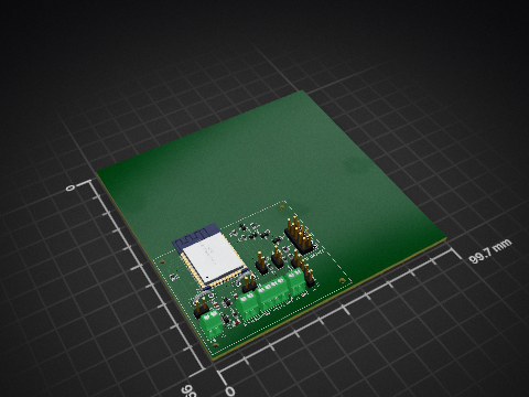
makehackvoid/ESP8266Lib
I decided to make a PCB for my ESP32 things. I have many installed, each made differently. It is time to standardise them, hence this KiCAD (6) project. ======

vitaliy-bobrov/avr-transistor-tester
Component/Transistor tester based on famous AVR Transistor Tester

AnhadSawhney/MechanicalKeyCalculator
These are the CAD files for a calculator with mechanical keyswitches.


arijitdasgupta/talisman
A simple Raspi Pico based dev board of sorts, with a SSD1306 screen & 3 buttons


Yes. The symbol is Pinmap_Generic:Q_PMOS_1G_2S_3D and the footprint Package_TO_SOT_SMD:SOT-23, both drawn on this page. PCBKit places them on a board for you when you design with it.
SOT-23, with 3 pins. Its footprint is drawn on this page.
Diodes Incorporated publishes it: the Datasheet link on this page opens it.
JLCPCB lists it as part C177033, with 6,537 in stock; the sellers' links on this page open their listings.
Parts like it in the library: the AO3400A by Alpha & Omega Semiconductor, the AO3400A by UMW, the AO3400 by Guangdong Hottech and the AO3400 by FOSAN. Check their datasheets: a part that fits the footprint may still differ in its ratings.
24 boards in 20 repositories on GitHub; the most starred are listed on this page, with their KiCad files.