2 layers78.7 × 70.5 mm
SerialTransmitter
zledtriac/74hc-uart
An asynchronous serial transmitter and receiver with 74hcxxx ICs
42 parts1MIT

 zledtriac/74hc-uart1
An asynchronous serial transmitter and receiver with 74hcxxx ICs
SerialReceiver is an open-source printed circuit board by zledtriac, from the zledtriac/74hc-uart repository on GitHub, published under the MIT licence. It is a 2-layer board of 78.7 × 70.5 mm with 46 parts on 69 nets, routed with 487 tracks and 23 vias.
It is built around the 74HC191S, 74HC132D and 74HC595, with the 74HC74D among its other parts. Its parts include 10 resistors, 9 capacitors, 6 ICs, 6 connectors and 5 diodes.


This is the transmitter. It's only consists of 6 ICs. Actually 5 because U6 the 74HC244 IC can be left out, but with the current configuration it can be operated manually for demonstrations.
The transmitter transmits the data with 1 start bit, 8bit data without parity and 1 stop bit on the end, with 9600 baud rate.
The transmitter has 3 pin headers for selecting the mode of operation (J3, J5, J6), before powering the transmitter up, please check the jumper positions, because the transmitter can't operate in a circuit if the transmitter is in manual operation mode.
The transmitter needs a 5V power supply to work, the power pins can be found on the Control header (J4) pin 1 - VCC, pin 2 - GND. After powering up the transmitter, due to the random behaviour of the set-reset latch made with the U5D and U5C NAND gate (74HC132) and of the U3A and U3B (74HC74) D flip-flops, it is possible that the cicuit will transmit a random data on the output.
If this behaviour can cause issues in the target device, it is recommended to build an output enable circuit after the U3B pin 9 output, which can be controlled by a switch, delay circuit or from software if the transmitter is connected to a CPU.
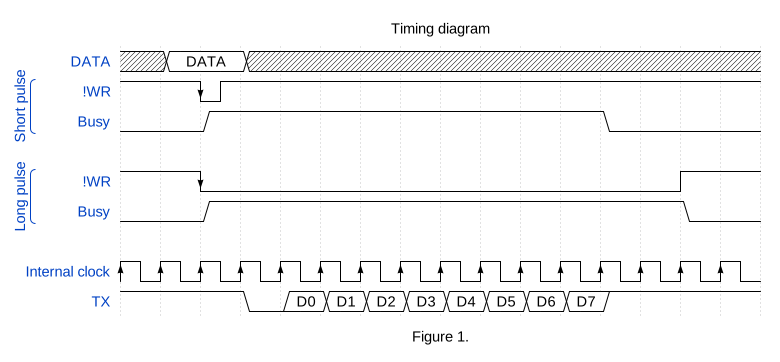
The Control header (J4) has two other pins for control, pin 5 - !WR, and pin 8 - Busy. The !WR is an active-low input and this input starts the data transmission. The Busy is an output which will be held high while the transmission is going (Short pulse section on Figure 1.), or while the !WR input is held low (Long pulse section on Figure 1.).
To send data, first set the data on the Data header (J1) then send a low pulse on the !WR pin. This will trigger the Input trigger circuitry. In this stage the output of the U5D will turn high, but since the U3A D flip-flop is not set, the inverted output of the U3A D flip-flop is also high, this will set the output of the U4A NAND gate to low, this will enables the load pins of the U1 (74HC165) shift register and the U2 (74HC191) counter IC, so the data will be loaded into the U1 shift register and the U2 counter IC will be set to 0. There is an extra bit made by the U4B NAND gate and the U3B D flip-flop, in the loading process it will set to one, this extra bit is the START bit. Since the U3A D flip-flop's clock input is connected to the main clock signal, the U3A D flip-flop will set and the inverted output of the U3A D flip-flop will turn to low. After this, every clock pulse will shift out the data from U1 (74HC165) shift register, and increment the U2 (74HC191) counter until U2 (74HC191) counter reaches 8. When the U2 (74HC191) counter reaches 8, the counting will stop and if the !WR input is high, it will reset the Input trigger circuitry, and after this, one clock pulse is needed to reset the U3A D flip-flop. So when the next write pulse comes in, the whole process will repeat.
To use the circuit in a manual operation mode, set the jumper on the J3 pin header to bridge the 1-2 pins, and on the J5 pin header to bridge the 2-3 pins. This will enables the U6 (74HC244) output so the data set by the SW1 dip switch will be put on the DATA input, and it will connect the SW2 button to the !WR input. After the data set on the SW1 dip switch, the data sending can be initiated by pressing the SW2 button.
please note that if the circuit is in manual operation mode, the DATA input will be driven by the U6 (74HC244) output and the !WR input will connected to the SW2 button, so it can't be used in other circuits!
The oscillator is made out of two schmitt-triggered NAND gate of the U4 (74HC132) IC. With the 10nF C7 capacitor and the 10kOhm R5 plus the 10kOhm RV1 trimmer potentiometer this oscillator can be adjusted between 6kHz and 12kHz. The oscillator's frequency is equal to the baud rate, so for the 9600 baud rate set the oscillator to 9.6kHz. For the tuning, a simple digital multimeter with frequency measuring capability is enough.
| Qty | Value | Footprint | References |
|---|---|---|---|
| 7 | 100nF | Capacitor_THT:C_Disc_D3.0mm_W2.0mm_P2.50mm | C2, C3, C4, C5, C6, C8, C9 |
| 4 | 1k | Resistor_THT:R_Axial_DIN0207_L6.3mm_D2.5mm_P10.16mm_Horizontal | R3, R5, R6, R7 |
| 3 | 10k | Resistor_THT:R_Axial_DIN0207_L6.3mm_D2.5mm_P10.16mm_Horizontal | R1, R2, R4 |
| 3 | LED | LED_THT:LED_D3.0mm | D1, D2, D3 |
| 2 | 15V | Diode_THT:D_DO-35_SOD27_P7.62mm_Horizontal | D4, D5 |
| 2 | 2N7000 | Package_TO_SOT_THT:TO-92_Inline_Wide | Q1, Q2 |
| 2 | 74HC191 | Package_DIP:DIP-16_W7.62mm | U2, U3 |
| 1 | 100uF | Capacitor_THT:CP_Radial_D6.3mm_P2.50mm | C7 |
| 1 | 10k | Potentiometer_THT:Potentiometer_Bourns_3296W_Vertical | RV1 |
| 1 | 20k | Resistor_THT:R_Axial_DIN0207_L6.3mm_D2.5mm_P10.16mm_Horizontal | R10 |
| 1 | 4k7 | Resistor_THT:R_Axial_DIN0207_L6.3mm_D2.5mm_P10.16mm_Horizontal | R8 |
| 1 | 510 | Resistor_THT:R_Axial_DIN0207_L6.3mm_D2.5mm_P10.16mm_Horizontal | R9 |
| 1 | 560pF | Capacitor_THT:C_Disc_D3.0mm_W2.0mm_P2.50mm | C1 |
| 1 | 74HC132 | Package_DIP:DIP-14_W7.62mm | U1 |
| 1 | 74HC595 | Package_DIP:DIP-16_W7.62mm | U4 |
| 1 | 74HC74 | Package_DIP:DIP-14_W7.62mm | U5 |
| 1 | 74LS244 | Package_DIP:DIP-20_W7.62mm | U6 |
| 1 | CONTROL | Connector_PinHeader_2.54mm:PinHeader_1x08_P2.54mm_Horizontal | J2 |
| 1 | Clock select | Connector_PinHeader_2.54mm:PinHeader_1x04_P2.54mm_Vertical | J4 |
| 1 | DATA | Connector_PinHeader_2.54mm:PinHeader_1x08_P2.54mm_Horizontal | J1 |
| 1 | HDSP-4830_2 | Package_DIP:DIP-20_W7.62mm_Socket | BAR1 |
| 1 | LED enable | Connector_PinHeader_2.54mm:PinHeader_1x03_P2.54mm_Vertical | J5 |
| 1 | Mode select | Connector_PinHeader_2.54mm:PinHeader_1x04_P2.54mm_Vertical | J6 |
| 1 | RX | Connector_PinHeader_2.54mm:PinHeader_1x02_P2.54mm_Horizontal | J3 |
| 1 | R_Network08 | Resistor_THT:R_Array_SIP9 | RN1 |
| 1 | SW_Push | Button_Switch_THT:SW_PUSH_6mm | SW1 |
The 42 most common of 46 parts.
zledtriac/74hc-uart
An asynchronous serial transmitter and receiver with 74hcxxx ICs


felipesantiagoach-ops/cdp1802-8bit-computer
8-bit microcomputer based on the RCA CDP1802, the first CMOS microprocessor. Three stages designed in KiCad: two built and tested (assembly programs, UART, Tiny BASIC, Elf/OS) and a final design with an ADC, I²C/SPI…


ladmanj/aymbedded
PCB for embed the AY-3-8910 and class-D amplifier into the ZX Spectrum+ case 2023/2024 Jakub Ladman (ladmanj at volny cz)


It measures 78.7 × 70.5 mm and has 2 copper layers, 1.6 mm thick.
46 parts, built around the 74HC191S, 74HC132D, 74HC595 and 74HC74D. The full list of its parts is on this page, with links to each part's symbol and footprint where PCBKit's library has them.
From the zledtriac/74hc-uart repository on GitHub, at the commit this page was made from: the board is hardware/receiver/SerialReceiver.kicad_pcb and its schematic hardware/receiver/SerialReceiver.kicad_sch. PCBKit opens the board in the browser, with nothing to install.
Its repository publishes it under the MIT licence: you may reuse it on that licence's terms (keep the author's notice, and for a copyleft licence share your changes alike).