
2 layers90 × 56.8 mm

A famicom discrete logic mapper
V0b is an open-source printed circuit board by smaldragon, from the smaldragon/BNUY-ROM repository on GitHub, published under the Unlicense licence. It is a 2-layer board of 93 × 58.4 mm with 39 parts on 113 nets, routed with 1,444 tracks and 208 vias.
It is built around the SAM2695, 74HC191S and 74HC139D, with the 74HC174D and 74HC670P-E among its other parts. Its parts include 17 capacitors, 10 ICs, 4 resistors, 1 diode and 1 crystal.


BNUY-ROM is an homebrew discrete logic mapper for the famicom/nes, which aims to have a similar level of capabilities to common ASIC mappers, while keeping a relatively low chip count. The mapper is designed to be modular, with features that can be included or ommitted depending on the needs of a game. It is similar to BNROM, hence the name.
Its capabilities are:
As an in-development mapper, there is currently no iNES number attributed, nor mainstream emulator support.
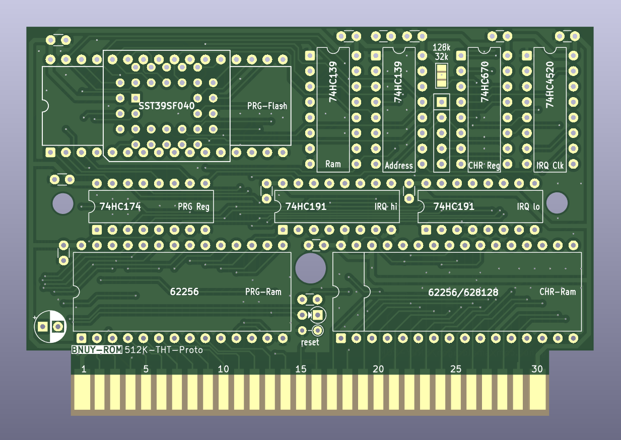
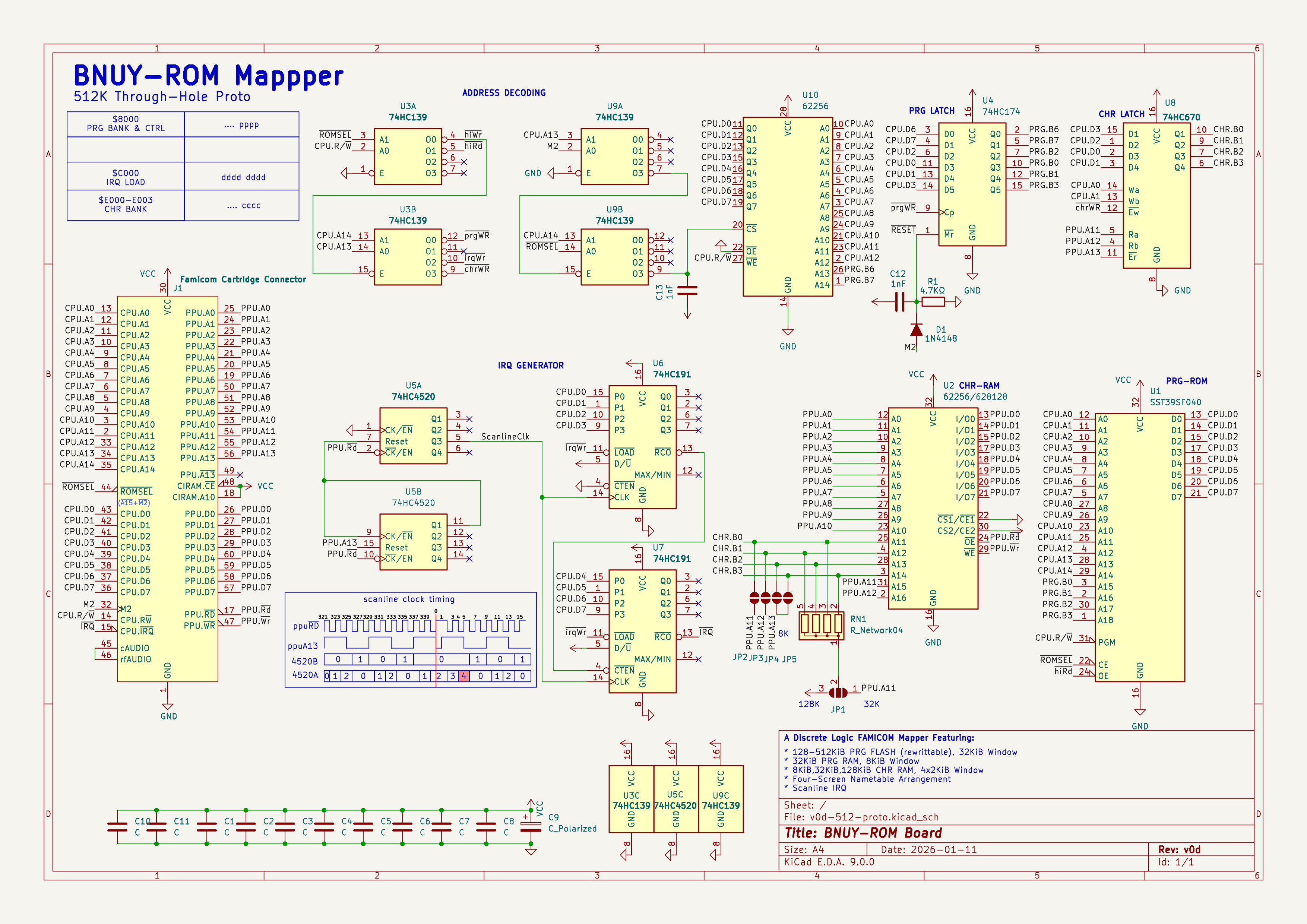
Render/schematic for the prototype tht version:
This register controls the banking of PRG Flash and Ram.
A~100x xxxx xxxx xxxx ($8000)
D~7654 3210
  ---------
  RRPP PPPP
  ||++-++++--- PRG-Flash Bank
++-----------PRG-Ram BankIn previous iterations of the design, this area was used for a SAM2695 soundchip. It is now unused and avaliable for potential mapper additions.
This register will load a value into a scanline counter, which decrements once per active scanline at ppu cycle 4. The counter will continuously trigger an IRQ whenever its value is 0.
There is no mechanism to stop the counter, and it will underflow to 255 if an interrupt is ignored for 1 scanline. To stop the generator from firing, a value of 255 should be written every nmi.
A~110x xxxx xxxx xxxx ($C000)
D~7654 3210
  ---------
  IIII IIII
++++-++++- 8-bit scanline counter valueThe 8-bit down counter is clocked by bit 2 of a prescaler counter, which increments on PPU reads with A13=1 and is cleared to zero on reads with A13=0. Normally one clock signal is generated by the prescaler per active scanline (including the pre-render scanline), but manual reads from PPU_DATA during VBlank or disabling rendering mid-frame will destabilize it. This can be overcome by reading once from A13=0 and twice from A13=1, followed by reloading the counter.
Overall the mechanism is similar to MMC5's scanline counter, but using relative values like the MMC3. Unlike the MMC3, this counter allows sprites to freely use either pattern table, including both while in 8x16 mode, and its timing simplifies scroll splits on consecutive scanlines.
It uses a x4520 to detect scanlines, and either a x40103 or two x191/x193s to hold the counter value.
If present, these registers select one of 16 2KiB CHR-RAM banks, to use for each of the 4 PPU pattern table windows.
In 8k/linear mode, the banking register is ommited. 16KiB of RAM are mapped to the PPU Address space, including 3840 bytes of "bonus ram" above the nametables, which the CPU may use to store values.
In 32K/shared mode, Banks 0 and 15 are shared with the 4 nametables, and should be avoided unless special care is taken. This leaves 14 banks that can be freely distributed across the 4 windows.
In 128K/independent mode, the register is still 4 bits wide, but now each window has their own unique set of 16 banks (by connecting the top 2 address lines of memory to ppu A11/A12), this effectively quadruples the amount of avaliable chr-ram without adding a second register chip to the board. The first 2 windows share banks 15 with the nametables
A~111x xxxx xxxx xx00 ($E000)
	CHR Window 0
A~111x xxxx xxxx xx01 ($E001)
	CHR Window 1
A~111x xxxx xxxx xx10 ($E002)
	CHR Window 2
A~111x xxxx xxxx xx11 ($E003)
	CHR Window 3

D~7654 3210
  ---------
  .... BBBB
       ++++- CHR Bank Select
This uses a single x670 4x4 register. A second register could be added to the design for an oversize variant of 512KiB (shared) or 2048KiB (independent). A design with CHR-ROM could be used instead, at the cost of losing 4-screen nametable arrangement.
Flash programming is achieved by writing a specific sequence of command bytes to particular memory addresses, during this process flash memory cannot be read as normal, and conflicting mapper registers will have their values overwritten. As such, flash programming code must be run from the internal 2KiB console ram, and all interrupts must be disabled.
Flash writes operate by ANDing the written byte with the existing value in memory, with the only way to set a bit being by erasing an entire sector to $FF.
39SF commands listen to A0-14, which requires clobbering the IRQ Counter, while 29F commands listen only to A0-A11, allowing commands to fit in the unused $A000-$BFFF region.
For more information check the datasheet for your particular flash chip.
A~$8000 D~BANK
A~$D555 D~$AA
A~$AAAA D~$55
A~$D555 D~$A0
A~ADDR D~DATAA~$8000 D~BANK
A~$AAAA D~$AA
A~$A555 D~$55
A~$AAAA D~$A0
A~ADDR D~DATAA~$8000 D~BANK
A~$D555 D~$AA
A~$AAAA D~$55
A~$D555 D~$80
A~$D555 D~$AA
A~$AAAA D~$55
A~ADDR D~$3039SF0x0 uses uniform sectors of 4KiB,
A~$8000 D~BANK
A~$AAAA D~$AA
A~$A555 D~$55
A~$AAAA D~$80
A~$AAAA D~$AA
A~$A555 D~$55
A~ADDR  D~$30
29FxxxFT uses sectors of varying sizes depending on bank:
$8000-$9FFF, $A000-$BFFF, 16KiB sector at $C000-$FFFFThe end of a write or erase operation can be detected by reading any memory address in flash until the same value is returned twice (toggle bit method).
Software ID mode can be entered to detect the manufacturer, size and type of flash chip, allowing for the same rom file to be compatible with multiple board configurations. Software ID is entered using the following command sequences:
A~$8000 D~$00
A~$D555 D~$AA
A~$AAAA D~$55
A~$D555 D~$90A~$8000 D~$00
A~$AAAA D~$AA
A~$A555 D~$55
A~$AAAA D~$90Software ID mode is exited by writing $F0 anywhere in flash.
$B5 - 39SF010 (128KiB)$B6 - 39SF020 (256KiB)$B7 - 39SF040 (512KiB)$51 - 29F200FT (256KiB)$23 - 29F400FT (512KiB)$D6 - 29F800FT (1024KiB)$D2 - 29F160FT (2048KiB)Mapper ID: Unassigned
Flags 6 (nametable layout/flashing)
D~3210
  ----
  F0BM
  | |+-- Hard-Wired Arragement
  | |      0: Vertical / 4-screen
  | |      1: Horizontal
  | +--- Uses Flash Saves
  |        0: No
  |        1: Yes
  +----- 4-Screen Arrangement
           0: Hard-Wired (using CIRAM)
           1: 4-Screen (using CHR-RAM)
Most games will have %1010 here.
Flags 8 (submapper)
D~7654
  ----
  FICC
  ||++-- CHR Banking Mode
  ||        0: 8K/Linear (no banking)
  ||        1: 32K/Shared (all banks avaliable in every window)
  ||        2: 128K/Independent (all windows have unique sets of banks)
  |+---- Interrupt Generator
  |         0: No IRQ
  |         1: Has IRQ
  +----- Flash Memory Type
            0: 39SF0x0 (sizes of 128K, 256K, 512K)
            1: 29FxxxFT (sizes of 256K, 512K, 1024K, 2048K)
PRG-ROM, PRG-RAM and CHR-RAM size
Size should match the memory accessible on the board.
| Qty | Value | Footprint | References |
|---|---|---|---|
| 8 | C_Small | Capacitor_SMD:C_1206_3216Metric_Pad1.33x1.80mm_HandSolder | C3, C4, C5, C6, C7, C8, C9, C16 |
| 3 | 74HC191 | PCM_Package_DIP_AKL:DIP-16_W7.62mm_LongPads | U4, U5, U6 |
| 3 | SolderJumper_2_Open | Jumper:SolderJumper-2_P1.3mm_Open_RoundedPad1.0x1.5mm | JP2, JP3, JP4 |
| 2 | 10µF | Capacitor_THT:CP_Radial_D4.0mm_P1.50mm | C11, C15 |
| 2 | 1µF | Capacitor_THT:C_Disc_D3.0mm_W1.6mm_P2.50mm | C1, C2 |
| 2 | 22pF | Capacitor_THT:C_Disc_D3.0mm_W1.6mm_P2.50mm | C13, C14 |
| 1 | 100nF | Capacitor_THT:C_Disc_D3.0mm_W1.6mm_P2.50mm | C12 |
| 1 | 100Ω | PCM_Resistor_THT_AKL:R_Axial_DIN0204_L3.6mm_D1.6mm_P2.54mm_Vertical | R2 |
| 1 | 10Ω | PCM_Resistor_THT_AKL:R_Axial_DIN0204_L3.6mm_D1.6mm_P2.54mm_Vertical | R3 |
| 1 | 12M | Crystal:Crystal_HC49-4H_Vertical | Y1 |
| 1 | 1N4148 | Diode_THT:D_DO-34_SOD68_P2.54mm_Vertical_AnodeUp | D1 |
| 1 | 1nF | Capacitor_THT:C_Disc_D3.0mm_W1.6mm_P2.50mm | C17 |
| 1 | 1µF | Capacitor_THT:CP_Radial_D4.0mm_P1.50mm | C10 |
| 1 | 4.7K | PCM_Resistor_THT_AKL:R_Axial_DIN0204_L3.6mm_D1.6mm_P2.54mm_Vertical | R4 |
| 1 | 47KΩ | PCM_Resistor_THT_AKL:R_Axial_DIN0204_L3.6mm_D1.6mm_P2.54mm_Vertical | R1 |
| 1 | 62256 | Package_DIP:DIP-28_W15.24mm_LongPads | U8 |
| 1 | 74HC139 | PCM_Package_DIP_AKL:DIP-16_W7.62mm_LongPads | U2 |
| 1 | 74HC174 | PCM_Package_DIP_AKL:DIP-16_W7.62mm_LongPads | U3 |
| 1 | 74HC670 | PCM_Package_DIP_AKL:DIP-16_W7.62mm_LongPads | U7 |
| 1 | Famicom_Cartridge_Edge | famicom:Famicom Cartridge Edge Connector (long legs) | H1 |
| 1 | MCP1700 | Package_TO_SOT_THT:TO-92_Inline | U10 |
| 1 | NOSAM | Jumper:SolderJumper-2_P1.3mm_Open_RoundedPad1.0x1.5mm | JP1 |
| 1 | R_Network04 | Resistor_THT:R_Array_SIP5 | RN1 |
| 1 | SAM2695 | Smal:QFN-48-1EP_6x6mm_P0.4mm_EP4.2x4.2mm_HAND | U9 |
| 1 | SST39SF040 | PCM_Package_DIP_AKL:DIP-32_W15.24mm_LongPads | U1 |


zledtriac/74hc-uart
An asynchronous serial transmitter and receiver with 74hcxxx ICs

KITTY-6502/hardware
the KITTY is a 65c02 homebrew kit microcomputer designed around text mode graphics and cartridge media. It is fully open source, and uses exclusively in-production parts.

artemisamsx/artemisa
Schematics, PCB designs and HDL simulations to build a 8-bits MSX computer


goriponsoft/ESE2RAM-Cartridge
Implementation of ESE-RAM using only general-purpose logic ICs (naming: ESE-ESE-RAM/ESE2-RAM).
It measures 93 × 58.4 mm and has 2 copper layers, 1.2 mm thick.
39 parts, built around the SAM2695, 74HC191S, 74HC139D and 74HC174D. The full list of its parts is on this page, with links to each part's symbol and footprint where PCBKit's library has them.
From the smaldragon/BNUY-ROM repository on GitHub, at the commit this page was made from: the board is KiCad/old/v0b/v0b.kicad_pcb and its schematic KiCad/old/v0a/v0a.kicad_sch. PCBKit opens the board in the browser, with nothing to install.
Its repository publishes it under the Unlicense licence: you may reuse it on that licence's terms (keep the author's notice, and for a copyleft licence share your changes alike).