
4 layers234 × 84 mm
Main panel
google/mozc-devices
Circuit diagrams and firmware source code for Gboard DIY keyboards
234 parts3kApache-2.0

 yuburoll/PISIC7
42-44key row staggered split keyboard with GRIN inspired layout under 102mm pcb
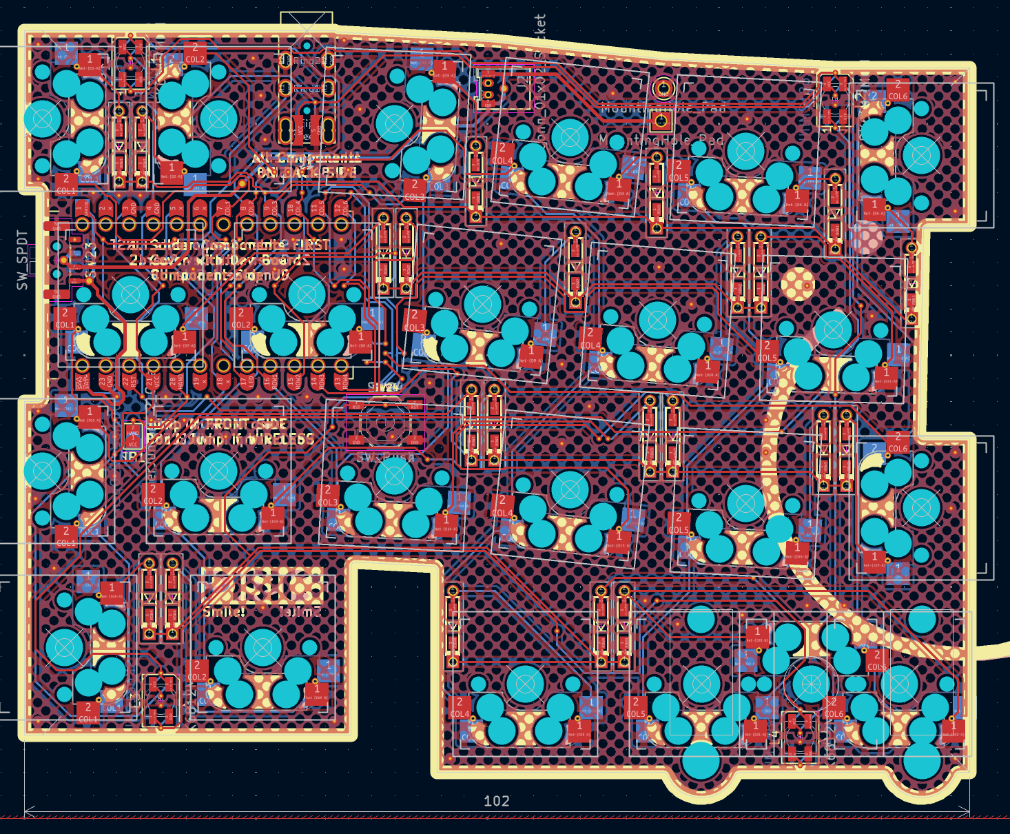
PISIC is an open-source printed circuit board by yuburoll, from the yuburoll/PISIC repository on GitHub, published under the MIT licence. It is a 2-layer board of 102 × 82.7 mm with 64 parts on 55 nets, routed with 737 tracks and 124 vias.
It is built around the SK6812MINI-E. Its parts include 26 switches, 22 diodes, 8 inductors, 2 connectors and 1 IC. It belongs with the keyboards and input boards and the AVR (ATmega, ATtiny) boards of this library.
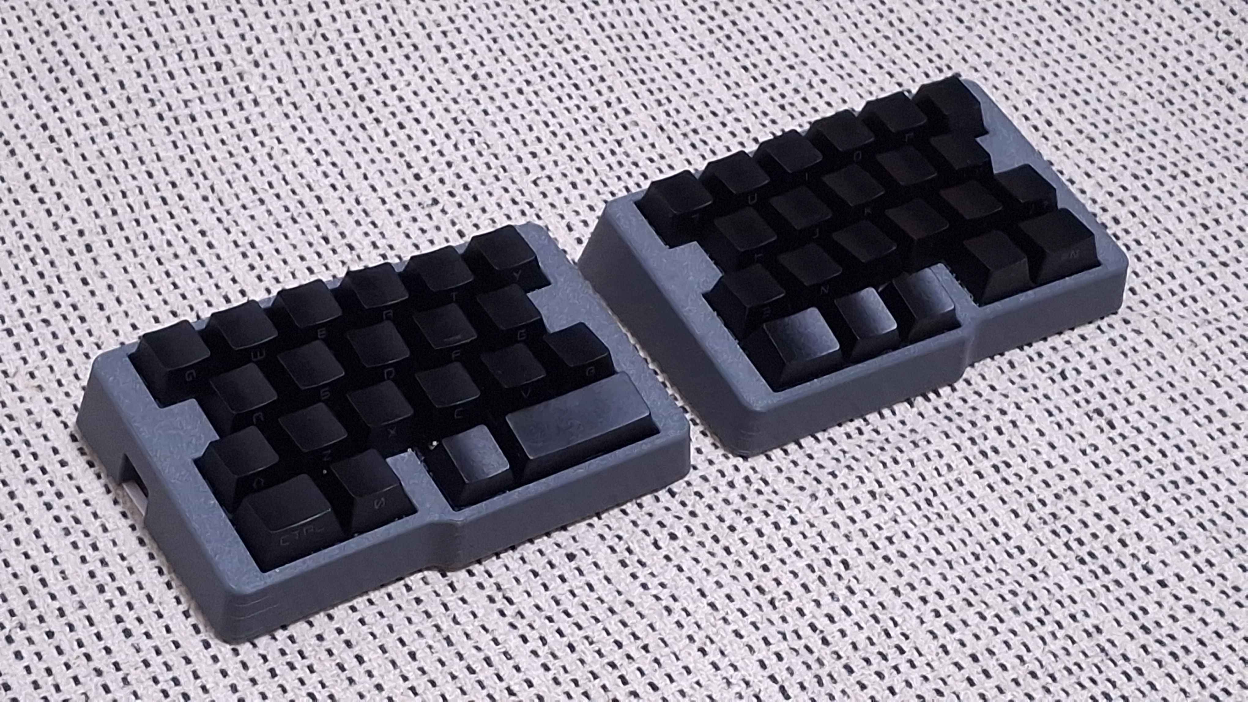
42-44key row staggered split keyboard with GRIN inspired layout, under 102mm PCB
The name PISIC means grin in korean, also is korean pun of grin layout of ansic.
2x pro micro form factor dev board
2x PISIC PCB Boards, provided from the repo
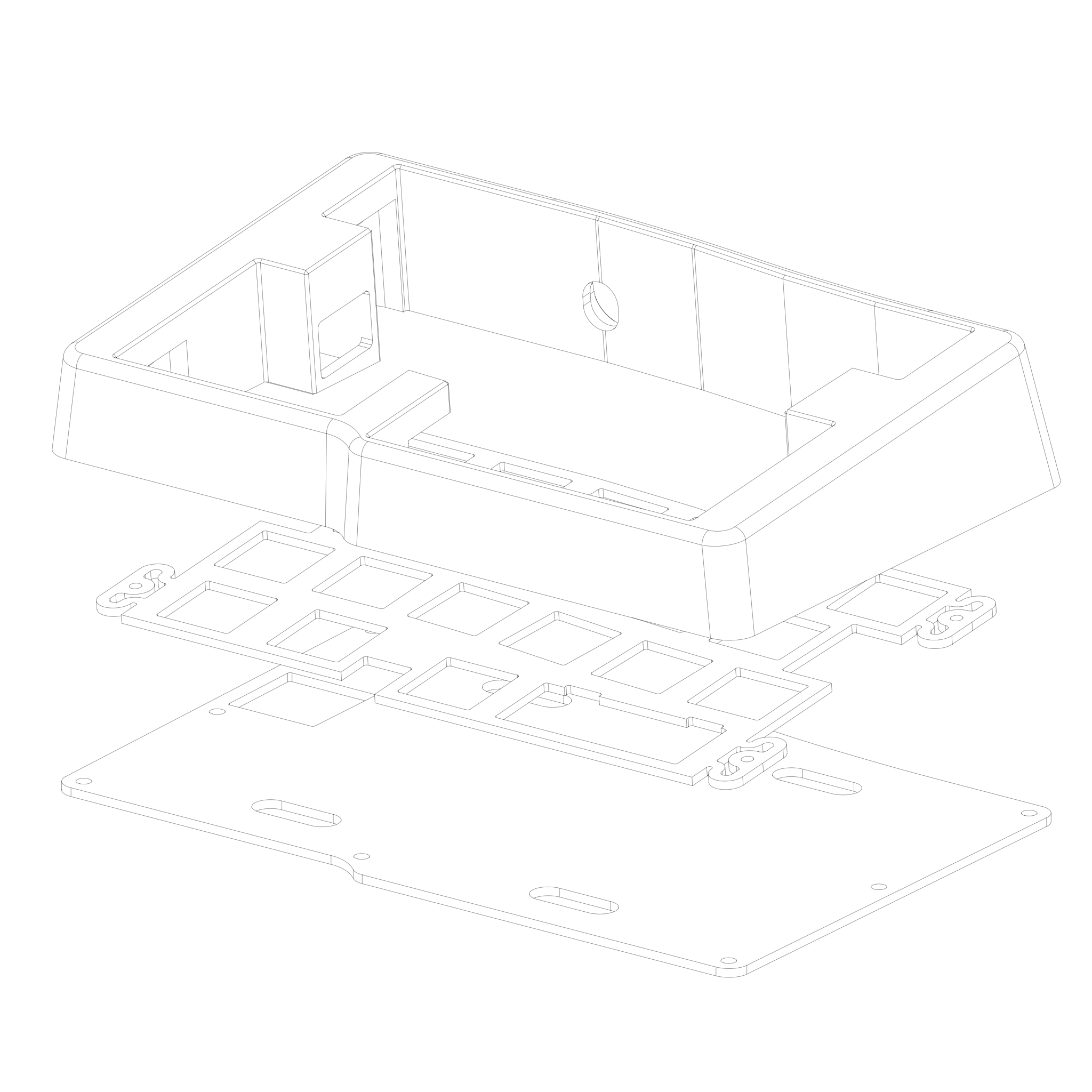
1x printed case sets, 2 parts total, provided from the repo
2x 1.5-1.6T keyboard plates, provided from the repo
2x 1.5-1.6T back plates, provided from the repo
44x diodes
46x Kailh hotswap sockets (or compatibles)
24x M2x6 screws, flathead
2x PJ320A 1/8(3.5mm) TRRS connector
2x 4x4x1.5mm surface mount tact switches (if needed)
8x SK6812 Mini or WS2812b Mini (3535) RGB LED (if wanted)
1x 1/8(3.5mm) TRRS cable
0-2x PCB Mounted 2u Keyboard Stabilizers, normally 1
42-44x MX Keyswitches, normally 43
8x 10mm bumpon stickers
A set of Keycaps
there's some notices before the build:
You may solder all hotswaps before soldering the dev board.
Assemble dev board with 2.5mm height pin headers on back side, assume that components side are faced up.
Jump every jumpers on front side.
Assemble Case-Plate-Switch first, not Plate-Switch-PCB.
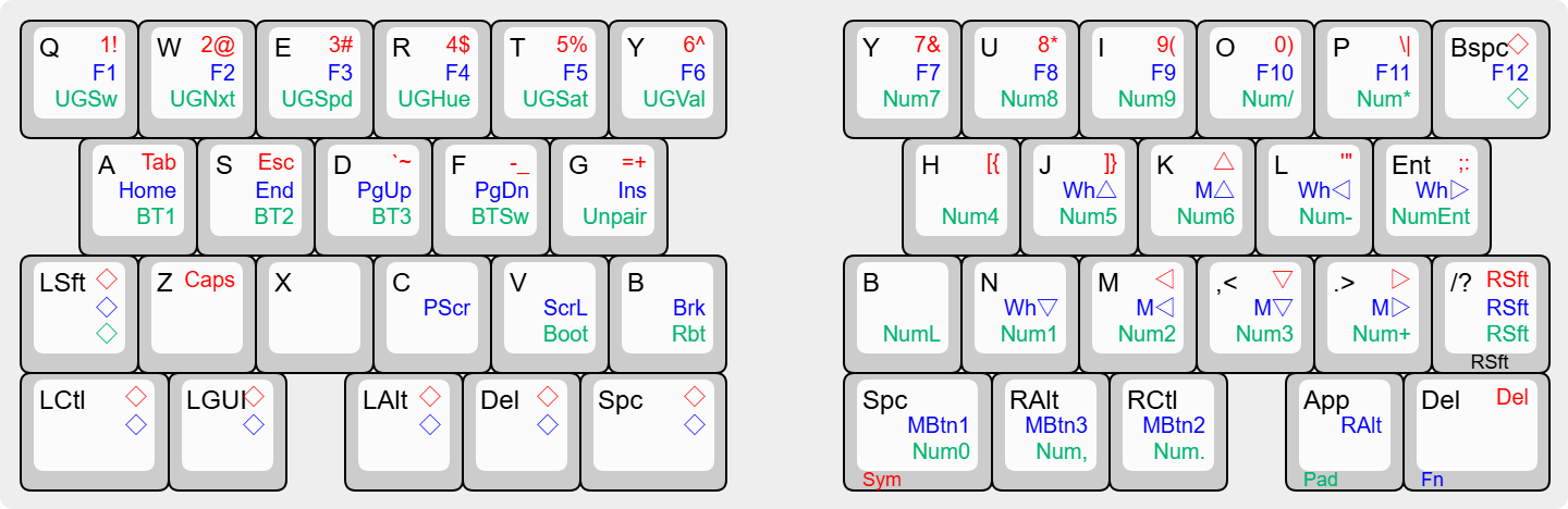
There are three more layers - Sym, Fn, Pad - which can be noticed by the color legends. ◇ Means Transparent; which uses base keymap.
Holding the color legend key swaps the layer.
all codes follow MIT license.
all designs and the hardware board follow CC BY-SA 4.0 license.
If you want to make a commercial product, it would be appreciated if you sponsor some bucks for me.
| Qty | Value | Footprint | References |
|---|---|---|---|
| 23 | SW_Push | yubuGadgetsFootpints:MX_Hotswap_FootprintPropertyFix_Guided | SW1, SW2, SW10, SW11, SW12, SW13, SW14, SW15, SW16, SW17, SW18, SW19, SW20, SW21, SW22, SW22 +7 |
| 22 | D | yubuGadgetsFootpints:Diode_TH_SMD_REVERSIBLE | D1, D2, D3, D10, D11, D12, D13, D14, D15, D16, D17, D18, D19, D20, D21, D22 +6 |
| 8 | SK6812MINI | LED_SMD:LED_SK6812MINI_PLCC4_3.5x3.5mm_P1.75mm | L1, L1, L2, L2, L3, L3, L4, L4 |
| 2 | SW_Push | Keebio-Parts:SW_SPST_TL3342 | SW24, SW24 |
| 2 | SolderJumper_2_Open | Jumper:SolderJumper-2_P1.3mm_Open_TrianglePad1.0x1.5mm | JP1, JP2 |
| 1 | AudioJack4 | yubuGadgetsFootpints:TRRS-PJ-320A-ReversiblePad | J1 |
| 1 | Conn_01x02_Socket | yubuGadgetsFootpints:Molex_PicoBlade_53048-0210_1x02_P1.25mm_Horizontal_ReversibleThru | J2 |
| 1 | MountingHole_Pad | TestPoint:TestPoint_THTPad_D2.0mm_Drill1.0mm | B-1 |
| 1 | MountingHole_Pad | TestPoint:TestPoint_THTPad_2.0x2.0mm_Drill1.0mm | B+1 |
| 1 | ProMicro_r | promicroReversiblePad:ProMicro_ReveribleThru_ComponentUp_OuterPad | U1 |
| 1 | SW_SPDT | yubuGadgetsFootpints:SW_SPDT_MSK12C02_Reversible | SW23 |
The 63 most common of 64 parts.
google/mozc-devices
Circuit diagrams and firmware source code for Gboard DIY keyboards

Bastardkb/Dilemma
The Dilemma is a vertical stagger low-profile keyboard with mods.

Pwnsat/FlatSat
Flatsat v1.0 is a hardware based platform for aerospace cybersecurity research

adamws/kicad-kbplacer
KiCad plugin for automatic keyboard's key placement and routing

imchipwood/dumbpad
Simple 4x4 numpad with rotary encoder. Powered by QMK via ATmega32u4 Pro Micro

makerforgetech/modular-biped
An open source framework for creating a bipedal modular companion robot.


It measures 102 × 82.7 mm and has 2 copper layers, 1.6 mm thick.
64 parts, built around the SK6812MINI-E. The full list of its parts is on this page, with links to each part's symbol and footprint where PCBKit's library has them.
From the yuburoll/PISIC repository on GitHub, at the commit this page was made from: the board is kicad/pisic.kicad_pcb and its schematic kicad/pisic.kicad_sch. PCBKit opens the board in the browser, with nothing to install.
Its repository publishes it under the MIT licence: you may reuse it on that licence's terms (keep the author's notice, and for a copyleft licence share your changes alike).