2 layers131.3 × 77.3 mm
ESP32 project
RatnakarSahooVSSUT/ESP32-Custom-PCB
Custom ESP32 development board designed in KiCad
70 parts

 yogesh8441/ESP32-CUSTOM-DEVELOPMENT-BOARD
A custom-designed ESP32-WROOM-32D Development Board developed using KiCad 10. This project demonstrates the complete PCB design workflow, including schematic design, PCB layout, routing, ground plane implementation…
ESP32 Project is an open-source printed circuit board by yogesh8441, from the yogesh8441/ESP32-CUSTOM-DEVELOPMENT-BOARD repository on GitHub. It is a 2-layer board of 118.4 × 61.2 mm with 63 parts on 85 nets, routed with 878 tracks and 94 vias.
It is built around the CH340C, ESP32-WROOM-32D and LM2596S-5.0, with the AP2112K-3.3, HDSP-7403 and SM518 among its other parts. Its parts include 18 resistors, 17 connectors, 14 capacitors, 5 ICs and 4 diodes. It belongs with the ESP32 boards of this library.


A custom-designed ESP32-WROOM-32D Development Board developed using KiCad 10. This project demonstrates the complete PCB design workflow, including schematic design, PCB layout, routing, ground plane implementation, ERC/DRC verification, and generation of manufacturing-ready Gerber files.
This development board is designed for embedded systems and IoT applications. The board integrates the ESP32-WROOM-32D module with USB programming, power regulation, communication interfaces, and peripheral connectors while following standard PCB design practices.
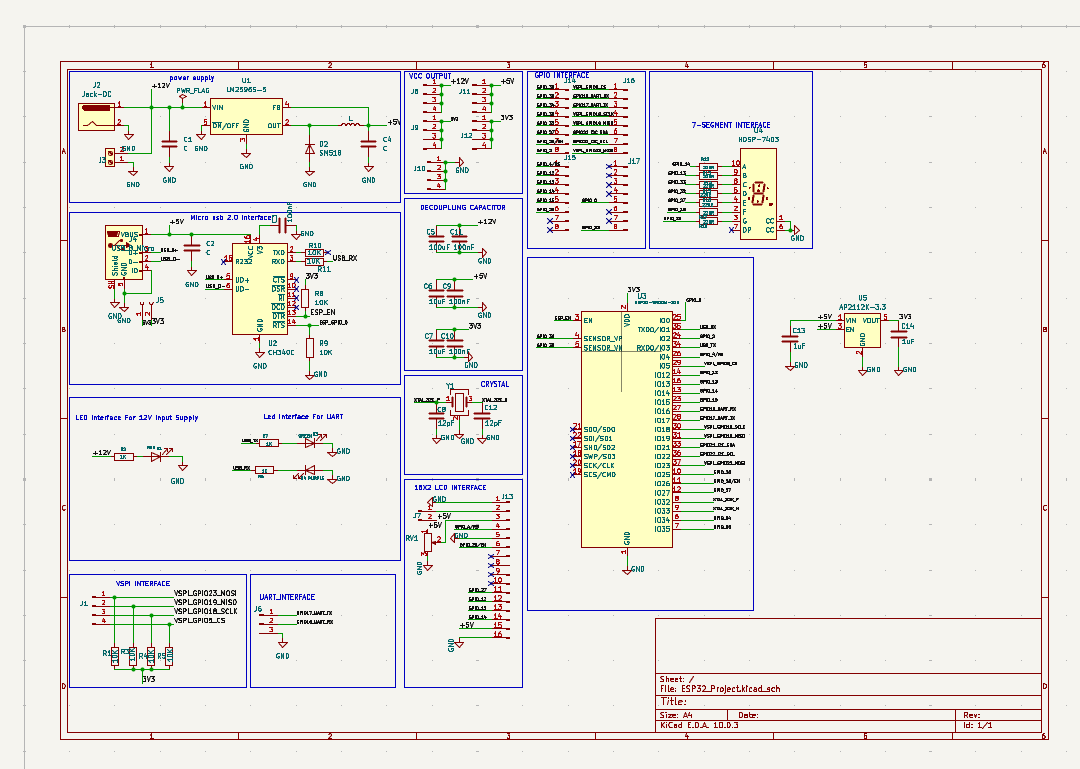
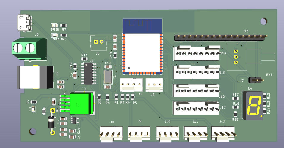
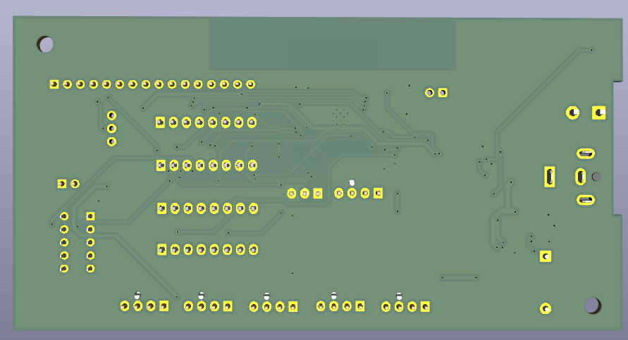
| Parameter | Specification |
|---|---|
| Microcontroller | ESP32-WROOM-32D |
| USB Interface | CH340C |
| Voltage Regulator | AP2112K-3.3 |
| PCB Layers | 2 |
| PCB Thickness | 1.6 mm |
| Copper Thickness | 1 oz |
| PCB Software | KiCad 10 |
| Manufacturing | JLCPCB Compatible |
ESP32-CUSTOM-DEVELOPMENT-BOARD/
│
├── Image/
│   ├── PCB_Top.png
│   ├── PCB_Bottom.png
│   └── Schematic.png
│
├── Schematic/
│   └── ESP32_Project.kicad_sch
│
├── PCB/
│   └── ESP32_Project.kicad_pcb
│
├── Gerber/
│   └── ESP32_Gerber.zip
│
├── Documents/
│
├── README.md
└── LICENSEThe generated Gerber files are manufacturing-ready and can be directly uploaded to PCB fabrication services such as:
Yogesh Kumar
| Qty | Value | Footprint | References |
|---|---|---|---|
| 8 | 10K | Resistor_SMD:R_0805_2012Metric | R1, R3, R4, R5, R8, R9, R10, R11 |
| 7 | 220R | Resistor_SMD:R_0805_2012Metric | R12, R13, R14, R15, R16, R17, R18 |
| 6 | Conn_01x04_Pin | Connector:FanPinHeader_1x04_P2.54mm_Vertical | J1, J8, J9, J10, J11, J12 |
| 4 | 100nF | Capacitor_SMD:C_0805_2012Metric_Pad1.18x1.45mm_HandSolder | C3, C9, C10, C11 |
| 4 | Conn_01x08_Pin | Connector_Molex:Molex_KK-254_AE-6410-08A_1x08_P2.54mm_Vertical | J14, J15, J16, J17 |
| 3 | 1K | Resistor_SMD:R_0805_2012Metric | R2, R6, R7 |
| 3 | C | Capacitor_SMD:C_0805_2012Metric_Pad1.18x1.45mm_HandSolder | C1, C2, C4 |
| 2 | 10uF | Capacitor_SMD:C_0805_2012Metric_Pad1.18x1.45mm_HandSolder | C6, C7 |
| 2 | 12pF | Capacitor_SMD:C_0805_2012Metric_Pad1.18x1.45mm_HandSolder | C8, C12 |
| 2 | 1uF | Capacitor_SMD:C_0805_2012Metric_Pad1.18x1.45mm_HandSolder | C13, C14 |
| 1 | 100uF | Capacitor_SMD:C_0805_2012Metric_Pad1.18x1.45mm_HandSolder | C5 |
| 1 | 10k | Potentiometer_THT:Potentiometer_Vishay_148-149_Single_Horizontal | RV1 |
| 1 | AP2112K-3.3 | Package_TO_SOT_SMD:SOT-23-5 | U5 |
| 1 | CH340C | Package_SO:SOIC-16_3.9x9.9mm_P1.27mm | U2 |
| 1 | Conn_01x02_Pin | Connector_PinHeader_2.54mm:PinHeader_1x02_P2.54mm_Vertical | J7 |
| 1 | Conn_01x02_Socket | Connector_Molex:Molex_SL_171971-0002_1x02_P2.54mm_Vertical | J5 |
| 1 | Conn_01x03_Pin | Connector:FanPinHeader_1x03_P2.54mm_Vertical | J6 |
| 1 | Conn_01x16_Pin | Connector_PinHeader_2.54mm:PinHeader_1x16_P2.54mm_Vertical | J13 |
| 1 | Crystal_GND24 | Crystal:Crystal_SMD_0603-4Pin_6.0x3.5mm | Y1 |
| 1 | ESP32-WROOM-32D | RF_Module:ESP32-WROOM-32D | U3 |
| 1 | GREEN | LED_SMD:LED_0805_2012Metric | D3 |
| 1 | HDSP-7403 | Display_7Segment:HDSP-7401 | U4 |
| 1 | Jack-DC | Connector_BarrelJack:BarrelJack_CUI_PJ-063AH_Horizontal | J2 |
| 1 | L | Inductor_SMD:L_0805_2012Metric_Pad1.05x1.20mm_HandSolder | L1 |
| 1 | LM2596S-5 | Package_TO_SOT_SMD:TO-263-5_TabPin3 | U1 |
| 1 | PURPLE | LED_SMD:LED_0805_2012Metric | D4 |
| 1 | RED | LED_SMD:LED_0805_2012Metric | D1 |
| 1 | SM518 | Diode_THT:D_DO-41_SOD81_P10.16mm_Horizontal | D2 |
| 1 | Screw_Terminal_01x02 | TerminalBlock_Phoenix:TerminalBlock_Phoenix_MKDS-1,5-2-5.08_1x02_P5.08mm_Horizontal | J3 |
| 1 | USB_B_Micro | Connector_USB:USB_Micro-B_Molex_47346-0001 | J4 |
The 61 most common of 63 parts.
RatnakarSahooVSSUT/ESP32-Custom-PCB
Custom ESP32 development board designed in KiCad


Saroja-J/ESP32-Board-
Custom ESP32-WROOM-32D PCB designed in KiCad with USB-UART,I2C,VSPI, and Sensor Interfaces.

Khoapham2004/ESP32-to-ESP-NOW-Control
The second repository contains the hardware design of the robot. It is mostly based on the 2025 version, with updated sensors, the BTS signal removed from the previous design, and a PCB that primarily uses SMD…


wenzel-lab/syringe-pumps-and-controller
Design of 3d printable syringe pumps and dual controller.

It measures 118.4 × 61.2 mm and has 2 copper layers, 1.6 mm thick.
63 parts, built around the CH340C, ESP32-WROOM-32D, LM2596S-5.0 and AP2112K-3.3. The full list of its parts is on this page, with links to each part's symbol and footprint where PCBKit's library has them.
From the yogesh8441/ESP32-CUSTOM-DEVELOPMENT-BOARD repository on GitHub, at the commit this page was made from: the board is ESP32_Project.kicad_pcb and its schematic ESP32_Project.kicad_sch. PCBKit opens the board in the browser, with nothing to install.
Its repository states no licence, so its author keeps all rights: ask yogesh8441 before reusing the design.