

2 layers70 × 60 mm

Converting a original Ericsson type 1951 to 4G
Carrier is an open-source printed circuit board by xecaz, from the xecaz/ericsson.type.1951.gsm.modding repository on GitHub. It is a 2-layer board of 44 × 100 mm with 21 parts on 13 nets, routed with 22 tracks and 0 vias.
It is built around the ESP32-DEVKITC-VE and AG1171. Its parts include 3 ICs, 2 capacitors and 2 connectors. It belongs with the ESP32 boards of this library.
A single-sided PCB that holds the three modules of the Ericsson 1951 → 4G/VoLTE build and breaks the phone's own parts out onto clearly-marked terminals. Sized as a tall strip, 44 × 100 mm, to fit a 45 × 120 mm mill bed.
| Ref | Part | Footprint |
|---|---|---|
| U1 | ESP32-DevKitC (38-pin) | 2×19, rows 25.4 mm apart, vertical |
| U2 | Silvertel Ag1171 SLIC | 14-pin SIL, vertical |
| U3 | Waveshare A7670E Cat-1 HAT (SKU 20049) | 2×20 RPi header, vertical |
| J1 | phone terminals | BELL · HOOK · DIAL · MIC · SPK (large pads) |
| J2 | PWR IN | 5V / GND |
| J3 | SLIC PWR | +VPWR (3.3–5 V) / GND |
| C1 | Ag1171 decoupling | ~100 µF electrolytic (+ 100 nF if you have room) |
| C2 | 5 V reservoir | ~1000 µF electrolytic (modem TX bursts) |
Modules solder onto male pins on top; all copper (traces + GND pour) is on the bottom (B.Cu). Every net is routed in copper except PWRKEY, one wire jumper.
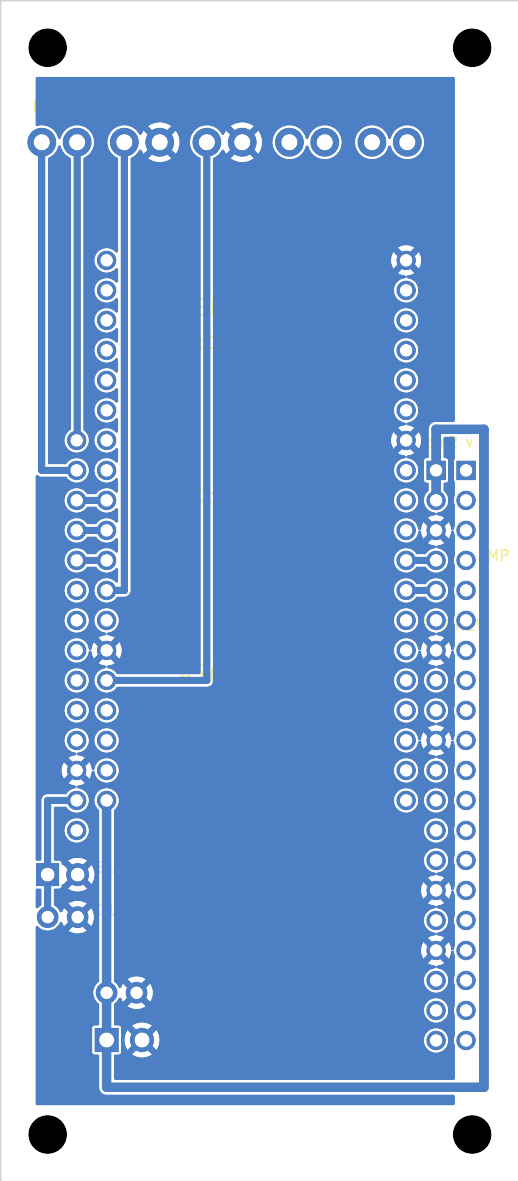
gerbers/carrier-gerbers.zip — send to the fab / load in your CAM (Gerber + drill)carrier.kicad_pcb — editable KiCad 10 board · gen_board.py — regenerate itcarrier.png — render · drc.rpt — design-rule reportESP_ROW = 22.86 at the top of gen_board.py and re-run.pin2 v mark
(the even-pin / 5 V row is nearest the ESP32).| Terminal | Pads | Goes to | Notes |
|---|---|---|---|
| BELL | TIP, RING | Ag1171 TIP/RING | drives the twin-gong bells (via the phone's own 1MF cap block) |
| HOOK | SIG, GND | ESP32 GPIO14 | hook switch to GND; firmware uses internal pull-up |
| DIAL | SIG, GND | ESP32 GPIO13 | rotary pulse contacts to GND; internal pull-up |
| MIC | 2 pads | modem mic | handset carbon mic — see audio note below |
| SPK | 2 pads | modem earpiece | handset receiver — see audio note below |
HOOK/DIAL are wired straight to GPIOs here (simplest, matches the RESEARCH.md "contacts to GPIO" route). If you'd rather sense them through the SLIC loop, wire them into the BELL/line loop and read the Ag1171 SHK line (already on GPIO27) instead.
| Net | ESP32 | A7670E HAT (Pi pin) | Ag1171 | On board |
|---|---|---|---|---|
| GND | GND | 6,14,20,30,34 | 12 GNDPWR | B.Cu pour |
| 5V | 5V (VIN) | 2, 4 | — | copper |
| +VPWR | — | — | 13 | copper (from J3) |
| TX | GPIO17 | 8 (→modem RXD) | — | copper |
| RX | GPIO16 | 10 (←modem TXD) | — | copper |
| PWRKEY | GPIO4 | 7 | — | wire jumper |
| F/R · RM · SHK | GPIO25/26/27 | — | 3 / 4 / 5 | copper |
| PD | — | — | 14 | left open (normal run) |
Wiring the modules together is not quite enough. The genuinely-needed extras:
Not needed: GPIO pull-ups (chose pull-up-capable pins), extra USB-C/CC resistors (those live on your charge module feeding PWR IN), or a boost — except note that the HAT wants 5 V, so a 1S pack needs a boost to 5 V into PWR IN (this revises the "modem on raw VBAT" note in the top-level CLAUDE.md, which was for a bare SIMCom module).
The A7670E's audio is on its 3.5 mm jack, not the 40-pin header — so it can't reach the handset through the board's module connector. Run a short 3.5 mm (TRRS) pigtail from the HAT jack to the MIC and SPK terminals (or wire the HAT's MIC±/EAR± solder pads). Those terminals are the handset's landing point; the modem side is your pigtail.
unconnected PWRKEY: the intentional jumper, not a fault.silk over copper / one isolated pour sliver: harmless on a poured 1-layer board.
| Qty | Value | Footprint | References |
|---|---|---|---|
| 14 | BELL, BELL, DIAL, DIAL, H, H, H, H, HOOK, HOOK, MIC, MIC, SPK, SPK | ||
| 1 | 1000uF | C2 | |
| 1 | 100uF | C1 | |
| 1 | A7670E-HAT | U3 | |
| 1 | Ag1171 | U2 | |
| 1 | ESP32-DevKitC | U1 | |
| 1 | PWR_IN | J2 | |
| 1 | SLIC_PWR | J3 |

sdylewski/Analog-Redial
A circuit board for old telephones to come back to life. Plug one or two phones in, and you can call the other phone, use bluetooth, connect to others via voip, and do a variety of other things with a plain old rotary…

harbaum/galagino
A Galaga, Pac-Man and Donkey Kong arcade emulator for the ESP32

RParkerE/OpenSilicon
OpenSilicon enables DIY semiconductor fabrication with open-source guides for building IC equipment at home. The project includes BOMs, 3D files, firmware, and PDKs, supporting makers and researchers in chip fabrication.

cole8888/SRNE-Solar-Charge-Controller-Monitor
Read data from SRNE solar charge controllers.


It measures 44 × 100 mm and has 2 copper layers, 1.6 mm thick.
21 parts, built around the ESP32-DEVKITC-VE and AG1171. The full list of its parts is on this page, with links to each part's symbol and footprint where PCBKit's library has them.
From the xecaz/ericsson.type.1951.gsm.modding repository on GitHub, at the commit this page was made from: the board is hardware/carrier-board/carrier.kicad_pcb. PCBKit opens the board in the browser, with nothing to install.
Its repository states no licence, so its author keeps all rights: ask xecaz before reusing the design.