
2 layers51.9 × 52 mm

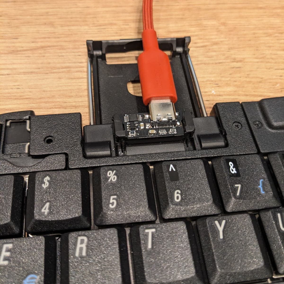
Palm™ Portable Keyboard USB adapter
Ppk is an open-source printed circuit board by wojtekka, from the wojtekka/ppk repository on GitHub. It is a 2-layer board of 26.8 × 10 mm with 13 parts on 19 nets, routed with 125 tracks and 9 vias.
It is built around the CH552E and SN74LVC1G00DBV. Its parts include 3 resistors, 2 capacitors, 2 ICs and 1 connector. It belongs with the keyboards and input and interfaces and adapters boards and the 8051 (CH55x, STC, AT89) boards of this library.


Based on CH552 Macropad mini by Stefan Wagner (https://github.com/wagiminator/CH552-Macropad-mini). Headers from the original code:
// ===================================================================================
// Project:   MacroPad Mini for CH551, CH552 and CH554
// Version:   v1.3
// Year:      2023
// Author:    Stefan Wagner
// Github:    https://github.com/wagiminator
// EasyEDA:   https://easyeda.com/wagiminator
// License:   http://creativecommons.org/licenses/by-sa/3.0/
// ===================================================================================

# Project:   chprog - Programming Tool for CH55x Microcontrollers
# Version:   v1.1
# Year:      2022
# Author:    Stefan Wagner
# Github:    https://github.com/wagiminator
# License:   MIT License
Based on Gist by Mightypork (https://gist.github.com/MightyPork/6da26e382a7ad91b5496ee55fdc73db2)
Key mapping compatible with https://github.com/pymo/ppk_bluetooth/
Hardware design released into public domain.
| Qty | Value | Footprint | References |
|---|---|---|---|
| 2 | 5k1 | Resistor_SMD:R_0805_2012Metric | R2, R3 |
| 1 | 100k | Resistor_SMD:R_0805_2012Metric | R4 |
| 1 | 100n | Capacitor_SMD:C_0805_2012Metric | C3 |
| 1 | 10u | Capacitor_SMD:C_0805_2012Metric | C4 |
| 1 | CH552E | Package_SO:MSOP-10_3x3mm_P0.5mm | U3 |
| 1 | DCD | TestPoint:TestPoint_Pad_1.5x1.5mm | TP1 |
| 1 | GND | TestPoint:TestPoint_Pad_1.5x1.5mm | TP5 |
| 1 | RTS | TestPoint:TestPoint_Pad_1.5x1.5mm | TP2 |
| 1 | RXD | TestPoint:TestPoint_Pad_1.5x1.5mm | TP3 |
| 1 | SN74LVC1G00DBV | Package_TO_SOT_SMD:SOT-23-5 | U1 |
| 1 | USB_C_Receptacle_USB2.0_16P | Connector_USB:USB_C_Receptacle_GCT_USB4110 | J1 |
| 1 | VCC | TestPoint:TestPoint_Pad_1.5x1.5mm | TP4 |
It measures 26.8 × 10 mm and has 2 copper layers, 1.6 mm thick.
13 parts, built around the CH552E and SN74LVC1G00DBV. The full list of its parts is on this page, with links to each part's symbol and footprint where PCBKit's library has them.
From the wojtekka/ppk repository on GitHub, at the commit this page was made from: the board is hardware/ppk.kicad_pcb and its schematic hardware/ppk.kicad_sch. PCBKit opens the board in the browser, with nothing to install.
Its repository states no licence, so its author keeps all rights: ask wojtekka before reusing the design.

KemalOeztuerk/STM32F446_Control_Board
STM32F446RET6 control board for UAV/robotics: CAN (SN65HVD230), hardware-inverted SBUS input, 4x PWM, 2x quadrature encoder, 4x ADC, SPI/UART/SWD headers — 2-layer KiCad design


acamilo/pcb-artwork-project
Collection of graphical PCBs containing memes, logos of youtube channels i watch, among other things.


kr-Eliza/tkey-open-hardware-reproduction
Reproducing the Tillitis TKey open hardware security key: 2-layer hand-solderable PCB, lab assembly and bring-up, Voltera prototype, SBOM

