Skip to the content
2 layers51.5 × 56 mmWeronika s hacktool, the printed circuit board in 3D

A Raspberry pi Pico based hardware tool that can be plugged in via USB-A or or a connecting wire between raspberry's pi pico and a device that you're connecting it to.
Size
51.5 × 56 mm
Copper layers
2
Thickness
1.6 mm
Parts
8
Nets
57
Pads
129
Tracks, vias
113, 16
Pours
2
Routed
Yes
KiCad
KiCad 10.0 (file 20260206)
Created
1 Jun 2026
Updated
15 Jun 2026

Overview

Weronika s hacktool is an open-source printed circuit board by weronikapad, from the weronikapad/weronika-s_hacktool repository on GitHub. It is a 2-layer board of 51.5 × 56 mm with 8 parts on 57 nets, routed with 113 tracks and 16 vias.

It is built around the TP4057. Its parts include 3 connectors, 1 resistor and 1 IC. It belongs with the RP2040 boards of this library.

Main components

1

README

README.md

Weronika's Hacktool

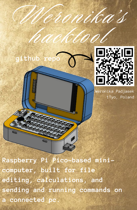
A Raspberry pi Pico based hardware tool that can be plugged in via USB-A or or a connecting wire between raspberry's pi pico and a device that you're connecting it to.

fallout_zine_template.pdf (6).png

3D model on onshape:

https://cad.onshape.com/documents/8ba63a7496dc739681835abf/w/b2486c84e183ee5c75462b5f/e/727d0ff90b4b33300ac8e23b?renderMode=0&uiState=6a1f47a38e48adf890f3cb43

Specifics

Raspberry pi pico is powered by a LiPo battery, that is charged through USB-A and the voltage that pico receives is controled by the power manager.

  1. specifics to connecting hardware parts a) battery:

    • connect it with a male to male wire to a connector pin socket 01x02

    b) keyboard (look at connector pins on conn_01x04 from KiCad view), (use female to female wires)
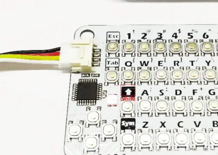
    • Pin1 -> wire -> the pin in the keyboard port that the black wire from the picture goes into
    • Pin2 -> wire -> the pin in the keyboard port that the red wire from the picture goes into
    • Pin3 -> wire -> the pin in the keyboard port that the white wire from the picture goes into
    • Pin4 -> wire -> the pin in the keyboard port that the yellow wire from the picture goes into keyboardspecifics

    c) screen (use female to female wires)(look at connector pins on conn_01x09 from KiCad view)
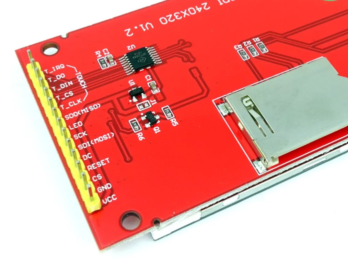
    • Pin1 -> wire -> vcc on the screen
    • Pin2 -> wire -> GND on the screen
    • Pin3 -> wire -> CS on the screen
    • Pin4 -> wire -> SDO(MISO) on the screen
    • Pin5 -> wire -> SCK on the screen
    • Pin6 -> wire -> SDI(MOSI) on the screen
    • Pin7 -> wire -> DC on the screen
    • Pin8 -> wire -> LED on the screen
backofscreen

Features

-Raspberry pi Pico -SD card port (microSD_HC_Molex_104031-0811) -USB-A (USB_A_CNCTech_1001-011-01101_Horizontal) -2000 Ohm resistor -Power manager (TP4057) -LCD display -Keyboard -LiPo Battery -Connectors on PCB for screen, keyboard and battery conection

PCB

Designed in KiCad, through pico's USB using REPL, pico can send commands to pluged pc and receive and print output, and through UART it can monitor traffic. Independently it can serve as a calculator or a text editor.

PCB's front copper layer view in KiCad
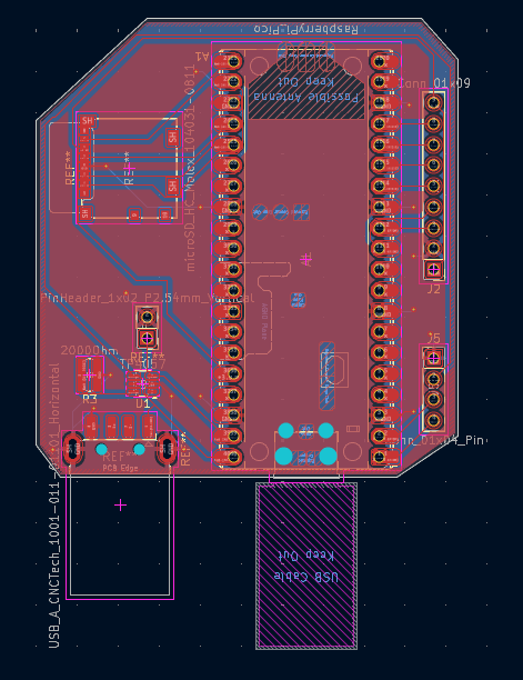
pcbfcu

PCB's back copper layer view in KiCad
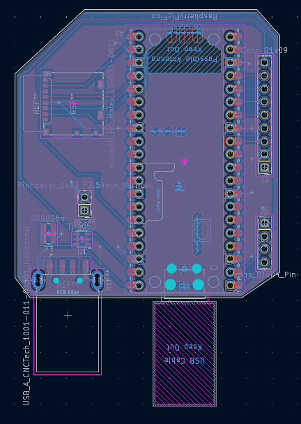
pcbbcu

PCB's 3D model, with exact location of specific connectors
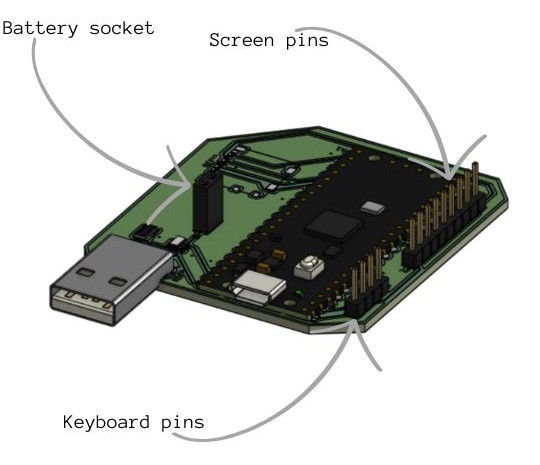
3dpcb.pdf

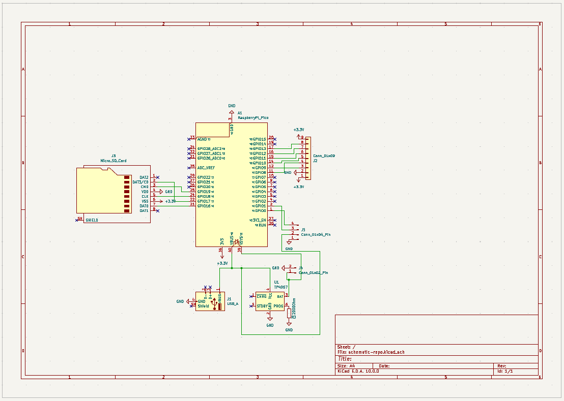
Schematic

Screenshot 2026-06-01 204912

detailed description on how to use

  1. download firmware for pico, and pc
  2. download Thonny
  3. works best with an sd card connected
  4. before assembling everything in the box:
    • plug raspberry pico via wire to your pc
    • push firmware files onto pico
  5. to stop any program at any time press esc
  6. in order to use the REPL program, or UART:
    • connect pico to at least the screen, and and keyboard a) for REPL:
      • in the terminal type "repl"
      • then type the command that you wish to run in your pluged device
      • pico is programed to always run in administrator mode in your pc's cmd so, in order for the rogram to run as intended you must allow it on your pc b) for UART: -in the terminal type "uart"
  7. to use the hacktool independently:
    • connect the pcb to keyboard, screen, and battery
    • charge the battery via USB-A a) to use the text editor:
      • type in the terminal "text" + your filename (it can be already saved on sd card or can be created by this command) if the file exists:
        • to edit the file type "edit"
        • to delete type "delete"
        • if you change your mind and you no longer wish to engage with the text editor type "leave" if it doesn't:
        • type "create" to create it and open it
        • type "leave" if you don't wish to create
  8. if you forgot any of those commands type "help" in the main terminal

why i build this:

I wanted to understand computers and cybersecurity better, i specifically used REPL as i thought it is one of the most universal hacking abilites of raspberry pi pico, I first decided uppon pico because it was all over my feed on tiktok but as it actually turns out it was the perfect fit for my project

credits:

image from the magazine page, originally distributed by kylatcarter on pinterest: https://pl.pinterest.com/pin/1135399756078582773/ readme structure inspired by notaroomba from github

Parts

8
QtyValueFootprintReferences
12000OhmResistor_SMD:R_0815_2038MetricR3
1Conn_01x02Connector_PinSocket_2.54mm:PinSocket_1x02_P2.54mm_VerticalJ6
1Conn_01x04_PinConnector_PinHeader_2.54mm:PinHeader_1x04_P2.54mm_VerticalJ5
1Conn_01x09Connector_PinHeader_2.54mm:PinHeader_1x09_P2.54mm_VerticalJ2
1RaspberryPi_PicoModule:RaspberryPi_Pico_Common_UnspecifiedA1
1TP4057Package_TO_SOT_SMD:TSOT-23-6U1

The 6 most common of 8 parts.

Similar boards

  • 6 layers55 × 95 mmEcho r1-rev1, the printed circuit board in 3D

    Echo r1-rev1

    amachronic/echoplayer

    Echo - Open Hardware Music Player

    154 parts281CERN-OHL-S-2.0
  • 2 layers285 × 94.6 mmKeyboard, the printed circuit board in 3D

    Keyboard

    Lotlab/Lot60-BLE-Keyboard

    A 60% bluetooth keyboard (Hardware)

    211 parts167CC-BY-SA-4.0
  • 2 layers18 × 14.4 mmBauble pcb, the printed circuit board in 3D

    Bauble pcb

    Spritetm/esp32c3-doom-bauble

    Christmas tree bauble with an ESP32C3 running Doom

    19 parts89
  • 4 layers72.4 × 44.4 mmBtmdpcb v04 eval, the printed circuit board in 3D

    Btmdpcb v04 eval

    17o2/bluetooth-minidisc

    Adding built-in bluetooth connectivity to a 20-year-old Mindisc player

    115 parts45
  • 4 layers75 × 36 mmEmoeNAP, the printed circuit board in 3D

    EmoeNAP

    Floyd-Fish/Noise-Amplifier

    An ultra-low noise amplifier to measure low-noise LDO/OPA's wide band output noise, and many other interesting measurements. Referred to AN-159.

    189 parts36GPL-3.0
  • 4 layers48 × 35.1 mmMicro esp32-s3, the printed circuit board in 3D

    Micro esp32-s3

    atomic14/esp32-tv-hardware

    This is Work In Progress - I'm still working on this.

    81 parts29
  • 2 layers30 × 30 mmBlewatch, the printed circuit board in 3D

    Blewatch

    jim-kirisame/LotWatch

    A BLE Watch using nrf51822

    27 parts22
  • 4 layers34.5 × 39 mmEpd watch, the printed circuit board in 3D

    Epd watch

    andr00d/epd_watch

    epd watch project

    63 parts18MIT

Questions

How big is the Weronika s hacktool PCB?

It measures 51.5 × 56 mm and has 2 copper layers, 1.6 mm thick.

What parts does the Weronika s hacktool use?

8 parts, built around the TP4057. The full list of its parts is on this page, with links to each part's symbol and footprint where PCBKit's library has them.

Where can I download the Weronika s hacktool KiCad files?

From the weronikapad/weronika-s_hacktool repository on GitHub, at the commit this page was made from: the board is hardware/hardware/hardware.kicad_pcb and its schematic hardware/hardware/hardware.kicad_sch. PCBKit opens the board in the browser, with nothing to install.

Can I use the Weronika s hacktool design in my own project?

Its repository states no licence, so its author keeps all rights: ask weronikapad before reusing the design.