
4 layers138.2 × 200.4 mm

 wdl1908/RC2014-front-panel-i2c
An I2C adapter board for the RC2014 Blue Box front panel.
Front panel i2c adapter is an open-source printed circuit board by wdl1908, from the wdl1908/RC2014-front-panel-i2c repository on GitHub, published under the CERN-OHL-W-2.0 licence. It is a 2-layer board of 64 × 27.7 mm with 27 parts on 33 nets, routed with 312 tracks and 36 vias.
It is built around the DS1233-5+T&R and TCA9555PWR(UMW). Its parts include 19 resistors, 3 connectors and 2 ICs. It belongs with the interfaces and adapters boards of this library.
An I2C adapter board for the RC2014 Blue Box front panel.
The RC2014 Universal Front Panel I/O Kit is one kit, but ships as two separate PCBs connected by a ribbon cable: the I/O Module (plugs into the RC2014 backplane, decodes I/O port 0, drives the LED/switch logic over the Z80 I/O bus, includes a DS1233 reset supervisor) and the Front Panel (the physical board carrying the actual 8 switches and 8 LEDs plus reset switch/power LED, no logic of its own).
This adapter replaces the I/O Module only. The Front Panel board is unchanged. This adapter's J1 is a female socket that mates directly onto the Front Panel board's own male header, board-to-board, no cable involved. It drives the same 8 switches/8 LEDs over I2C through a single TCA9555 16-bit I/O expander (one register bank for switch input, one for LED output) instead of the Z80 I/O bus board.
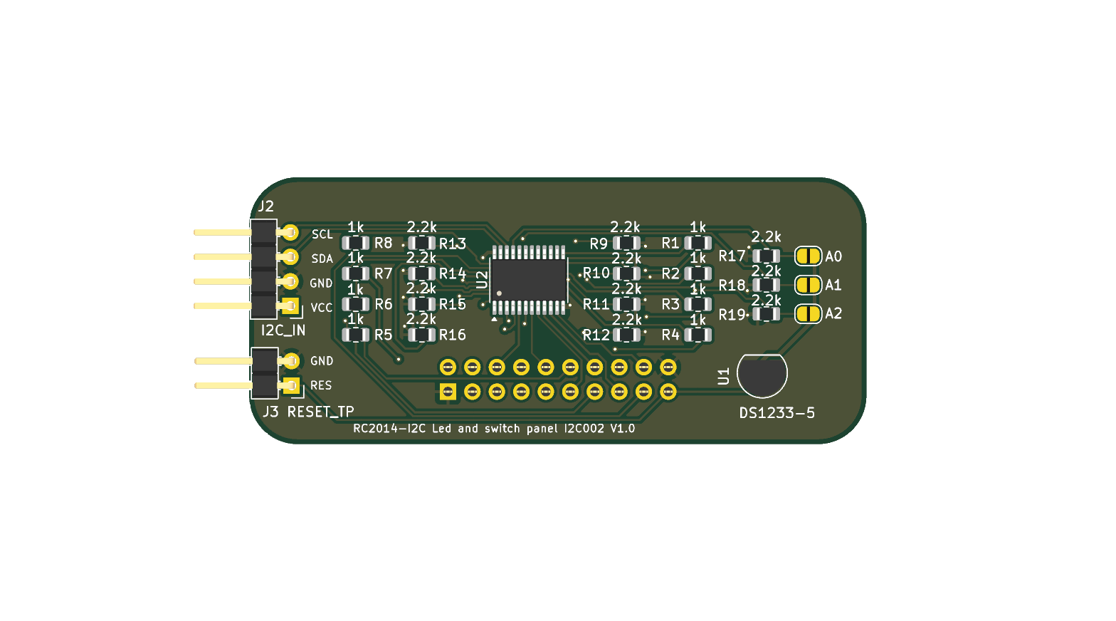
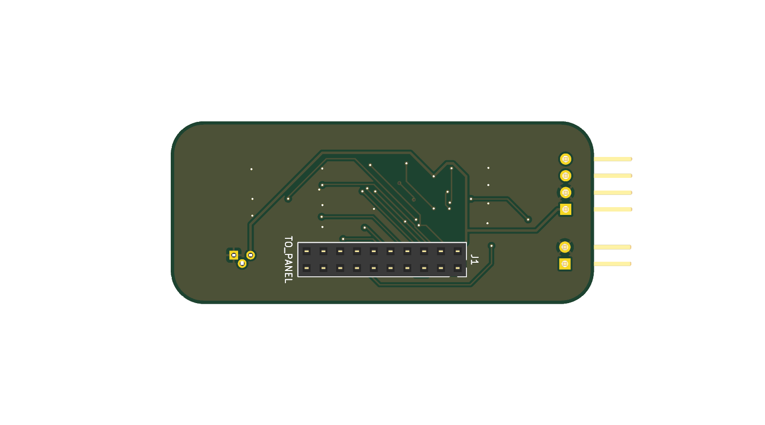
Real board photos (phone camera, lighting still a work in progress):
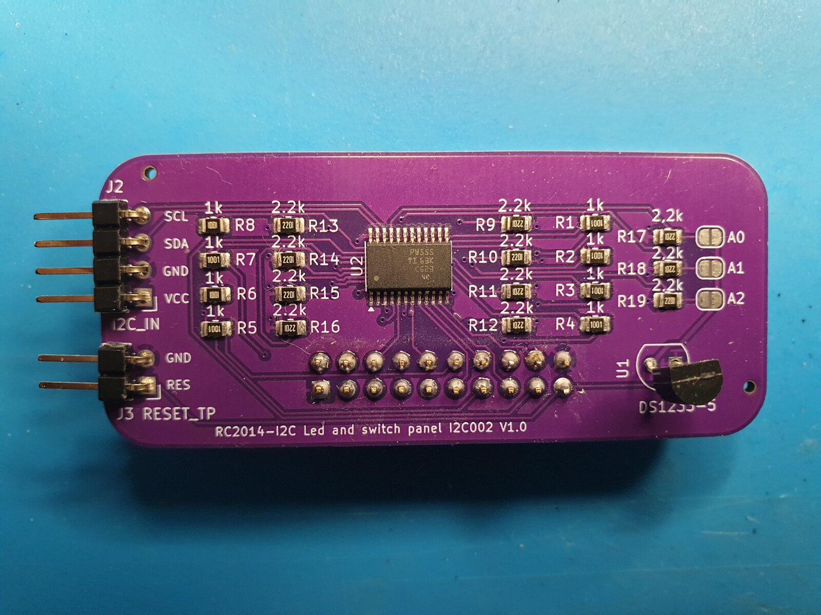
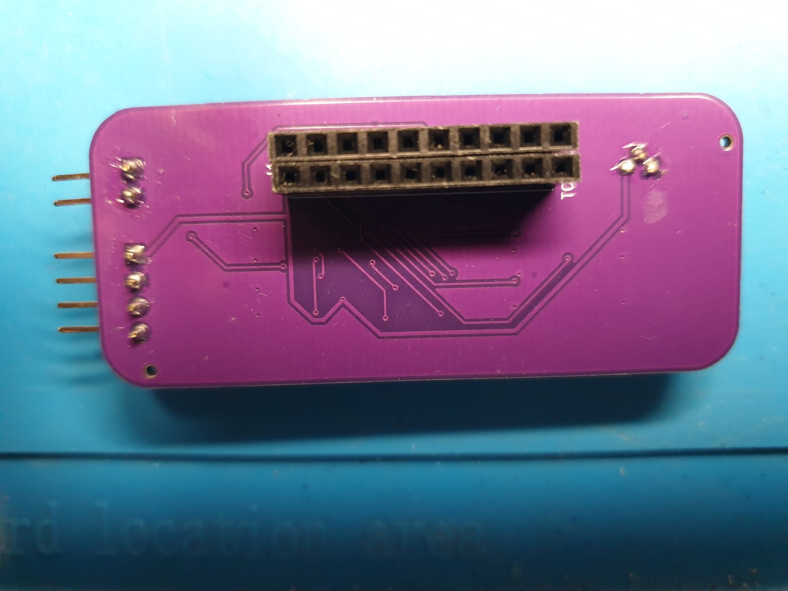
Note: z80kits also sells a larger "Blue Box Front Panel Kit for RomWBW" bundle, with the same two boards plus an LCD module and enclosure-specific parts for the Blue Box case. This adapter replaces the same I/O Module board in either kit.
Hardware-confirmed working, both directions (LEDs out, switches in),
including graceful degradation when the board is unplugged (system boots
fine without it, front panel simply reports not present). See kicad/ for
the full schematic/PCB source, fab/ for ready-to-order fabrication files,
and images/ for reference renders.
fab/ contains everything needed to order this board pre-assembled from
JLCPCB:
front_panel_i2c_adapter_gerbers.zip, board gerbers/drill filesfront_panel_i2c_adapter_bom_jlcpcb.csv, BOM in JLCPCB's SMT
assembly upload formatfront_panel_i2c_adapter_cpl.csv, component placement (CPL) file,
same upload flowUpload the gerbers zip under PCB, then the BOM + CPL pair under SMT
Assembly. Editable KiCad source (schematic + PCB + project + local
symbol/footprint libraries) is in kicad/.
I2C_IN), upstream I2C. 4-pin header, the board's only external
link to the bus: pin 1 VCC, pin 2 GND, pin 3 SDA, pin 4 SCL.RESET_TP), reset breakout, needs a wire. The board carries a
DS1233-5 reset supervisor, wired-OR onto the same Reset net as the Front
Panel board's manual reset switch (via J1 pin 19). That combined Reset
net is broken out to J3, a 2-pin header (RESET, GND). J3 is not wired to
anything else on the board. Run a wire from J3 to wherever the reset
switch's net is accessible on your backplane, RC2014 backplanes don't
expose ~RESET at the card-edge slots directly.0x20. Bridge the corresponding jumper(s)
to change the address, e.g. if you need more than one of this board on
the same bus.Front panel support over I2C requires a matching change to RomWBW's HBIOS
front panel driver (FP_DETECT/FP_SETLEDS/FP_GETSWITCHES). That driver
is written and hardware-confirmed against this board, but not yet published
upstream, still going through a final review pass.
Driver link: pending, will be added here once published.
Once the driver is available, these are the config values used to build RomWBW against this board (RC2014 Zed/Zed Pro target). This board is a plain I2C slave, it needs a working I2C bus master already on the system, either a real PCF8584 chip or the bitbang driver, not both:
| Setting | Value | Meaning |
|---|---|---|
I2CPCFENABLE | TRUE | Enable the PCF8584 I2C bus master (real chip). Mutually exclusive with I2CBITENABLE |
I2CBITENABLE | FALSE | Enable the bitbang I2C bus master (SC137) instead of a real PCF8584 chip. Mutually exclusive with I2CPCFENABLE, set this TRUE and I2CPCFENABLE FALSE if you don't have a PCF8584 |
FPLED_ENABLE | TRUE | Enable front panel LEDs |
FPSW_ENABLE | TRUE | Enable front panel switches |
FP_USE_I2C | TRUE | Drive the front panel over I2C instead of the Z80 I/O bus |
FP_I2CADR | $20 | TCA9555 7-bit I2C address, with A0/A1/A2 tied low (board default, adjust if you've jumpered a different address) |
FPLED_INV | FALSE (default) | TCA9555 output is active-high, no inversion needed |
LEDs and switches share the one TCA9555 chip/address. Register select (Port 0 = switches/input, Port 1 = LEDs/output) is handled by the driver, not a config option.
CERN-OHL-W v2 (CERN Open Hardware Licence, Weakly Reciprocal variant).
| Qty | Value | Footprint | References |
|---|---|---|---|
| 11 | 2.2k | Resistor_SMD:R_0805_2012Metric | R9, R10, R11, R12, R13, R14, R15, R16, R17, R18, R19 |
| 8 | 1k | Resistor_SMD:R_0805_2012Metric | R1, R2, R3, R4, R5, R6, R7, R8 |
| 3 | SolderJumper_2_Open | Jumper:SolderJumper-2_P1.3mm_Open_RoundedPad1.0x1.5mm | A0, A1, A2 |
| 1 | DS1233-5 | Package_TO_SOT_THT:TO-92 | U1 |
| 1 | I2C_IN | Connector_PinHeader_2.54mm:PinHeader_1x04_P2.54mm_Horizontal | J2 |
| 1 | RESET_TP | Connector_PinHeader_2.54mm:PinHeader_1x02_P2.54mm_Horizontal | J3 |
| 1 | TCA9555PWR | Package_SO:TSSOP-24_4.4x7.8mm_P0.65mm | U2 |
| 1 | TO_PANEL | RC2014_I2C:PinSocket_2x10_P2.54mm_Vertical | J1 |


Biacco42/modulo-ergo42
これは Beta バージョンの組み立てガイドです。Alpha 版は Alpha ブランチのドキュメントを参照してください。


lastlxrd/Pogopo
Open-source modular ESP32-S3 handheld console featuring custom hardware, a Sharp Memory LCD, pogopoOS, emulation, motion controls, audio, haptics, and expandable modules.

AnhadSawhney/MechanicalKeyCalculator
These are the CAD files for a calculator with mechanical keyswitches.

It measures 64 × 27.7 mm and has 2 copper layers, 1.6 mm thick.
27 parts, built around the DS1233-5+T&R and TCA9555PWR(UMW). The full list of its parts is on this page, with links to each part's symbol and footprint where PCBKit's library has them.
From the wdl1908/RC2014-front-panel-i2c repository on GitHub, at the commit this page was made from: the board is kicad/front_panel_i2c_adapter.kicad_pcb and its schematic kicad/front_panel_i2c_adapter.kicad_sch. PCBKit opens the board in the browser, with nothing to install.
Its repository publishes it under the CERN-OHL-W-2.0 licence: you may reuse it on that licence's terms (keep the author's notice, and for a copyleft licence share your changes alike).