PCB-focused multiphysics simulation, from board to complete assembly: PI, SI, circuits, thermal, EM/RF and mechanical workflows, with MCAD collaboration and a roadmap toward large-scale coupled assemblies.
Iot esp eth ind is an open-source printed circuit board by wayri, from the wayri/SPIKE repository on GitHub. It is a 4-layer board of 29.5 × 64.5 mm with 150 parts on 111 nets, routed with 2,603 tracks and 289 vias.
It is built around the 74AUP1G126GM, ESP32-D0WD and CH340G, with the W25Q128JVSIQ, 74AHC1G08GW and BAT54WS among its other parts. Its parts include 54 capacitors, 34 resistors, 28 diodes, 8 ICs and 7 inductors. It belongs with the radio and wireless and home automation and IoT boards and the ESP32 boards of this library.
This fixture pairs a 40 mm x 30 mm two-layer FR-4 patch board with one
explicit external dielectric object. The board copper and stackup are in
patch_with_radome.kicad_pcb; the radome is intentionally kept outside the
PCB file in antenna_with_radome_run.json so it can be passed as solver input.
bare_antenna_run.json and antenna_with_radome_run.json define a paired
bare-versus-radome experiment on exactly the same board, feed, frequency sweep,
and requested mesh size. The latter keeps parameters.surrounding_geometry
inline with the solver parameters.
For the radome case, its first corner is (95, 95, 10) mm and its dimensions
are (50, 40, 1.5) mm. The board occupies x=100..140 mm and y=100..130 mm.
The solver coordinate system uses the top copper as z=0; positive z points
into the air in front of the antenna. The slab therefore begins 10 mm above
the top copper and ends at 11.5 mm.
epsilon_r: 2.1 is an explicit fixture input. No loss tangent is present
because the current surroundings contract and EMerge adapter do not transfer
external dielectric loss. Do not use a lossless result to make radome
transmission, gain, pattern, or compliance claims.
The object uses the spike/emerge-surroundings/v1 contract:
This is a planar surrogate, not a curved radome or a complete vehicle,
enclosure, bracket, cable, connector, fastener, or ground-plane model. Any
comparison between the bare and radome cases still needs mesh convergence,
boundary checks, material characterization, and measurement correlation.
Reproduce and inspect the paired result
From the repository root with EMerge 3.0.0a19 installed in .venv-emerge3:
Both seven-frequency runs completed through SPIKE's isolated extension host
with model_status: unvalidated; their saved results are
bare_result.json and
covered_result.json. The
comparison_evidence.json checks identical board,
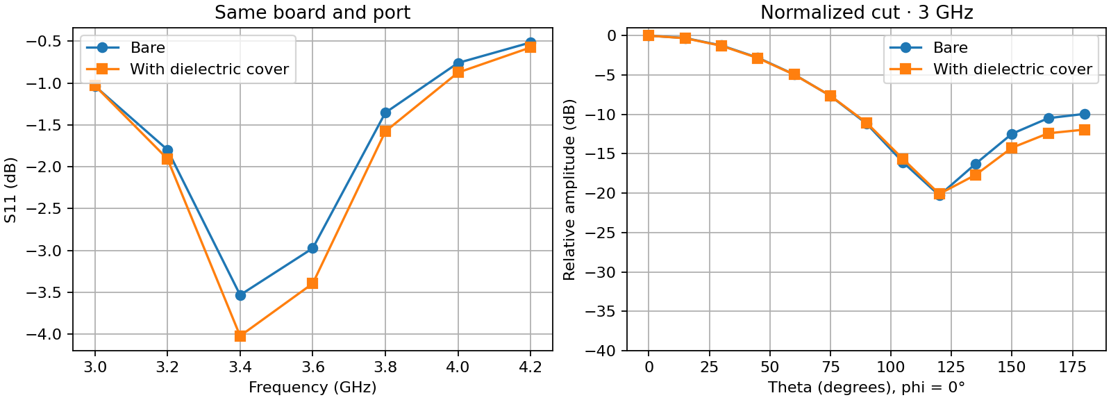
port, frequency and requested mesh inputs. At 3.4 GHz, S11 was -3.53 dB bare
and -4.02 dB covered. At 3 GHz, the independently peak-normalized relative
field sample at theta 180°, phi 0° changed from -9.94 to -11.93 dB. This
angular difference is a change in normalized pattern shape, not radome
insertion loss or absolute gain.
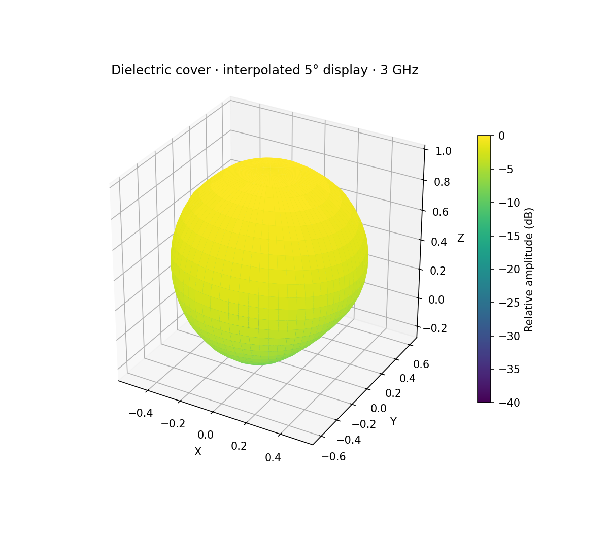
The paired S11 and angular-cut figure and
interpolated 3D covered pattern are saved
display artifacts. The 3D surface bilinearly interpolates relative linear
amplitude from the solver's 13 × 25 angular grid to 5° spacing. SPIKE offers
the same display interpolation, the original solved grid, and a relative
pattern overlay in the EMI chamber. Its bench can be shown, made translucent,
or hidden without changing the FEM case. None of those display choices creates
new solved field values.
PCB-focused multiphysics simulation, from board to complete assembly: PI, SI, circuits, thermal, EM/RF and mechanical workflows, with MCAD collaboration and a roadmap toward large-scale coupled assemblies.
Un système de réveil connecté qui combine une station audio, un bracelet de mouvement et une application mobile pour transformer le réveil en un vrai départ de journée.
Firmware & PCB for CAN Interface to a 28V DC Motor
86 partsMIT
Questions
How big is the Iot esp eth ind PCB?
It measures 29.5 × 64.5 mm and has 4 copper layers, 1.61 mm thick.
What parts does the Iot esp eth ind use?
150 parts, built around the 74AUP1G126GM, ESP32-D0WD, CH340G and W25Q128JVSIQ. The full list of its parts is on this page, with links to each part's symbol and footprint where PCBKit's library has them.
Where can I download the Iot esp eth ind KiCad files?
From the wayri/SPIKE repository on GitHub, at the commit this page was made from: the board is examples/esp32/source/iot-esp-eth-ind.kicad_pcb and its schematic examples/esp32/source/iot-esp-eth-ind-cpu.kicad_sch. PCBKit opens the board in the browser, with nothing to install.
Can I use the Iot esp eth ind design in my own project?
Its repository states no licence, so its author keeps all rights: ask wayri before reusing the design.