
2 layers22.2 × 46.4 mm
C64-Switchless Quad Kernal Switcher
bwack/C64-Switchless-Multi-Kernal-27C256-adapter
Kernal switcher for the C64/C64C/C128
14 parts112

 vindognz/project-luminescence
Project Luminescence is a custom heart shaped PCB with 10 red LEDs and a trimpot for analog brightness control.
Project luminescence is an open-source printed circuit board by vindognz, from the vindognz/project-luminescence repository on GitHub. It is a 2-layer board of 70 × 70 mm with 16 parts on 11 nets, routed with 76 tracks and 6 vias.
It is built around the ATTINY85-20PU. Its parts include 10 diodes, 2 switches, 1 resistor and 1 IC. It belongs with the AVR (ATmega, ATtiny) boards of this library.
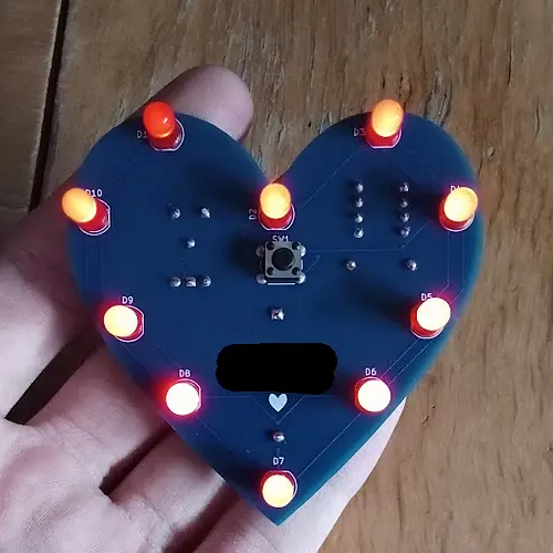
Project Luminescence is a custom heart shaped PCB with 10 red LEDs and a trimpot for analog brightness control.
Flip the switch on the back, then press the button on the front to cycle between off, on, and a slow fade mode. Use the trimpot on the back to tune the brightness.
I designed this as a birthday present for my girlfriend!
I opted for a pretty PCB instead of any form of case, so no 3D design files.
However, I was scared to omit this section, so cad/pcb.step is just the populated PCB, exported from KiCad.
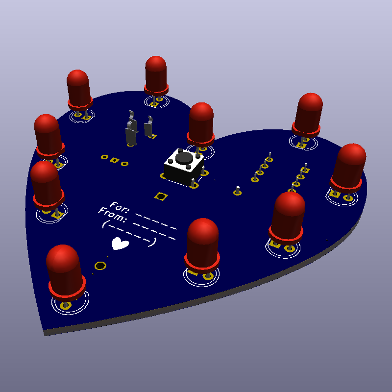
This is my PCB. I designed it in KiCad!
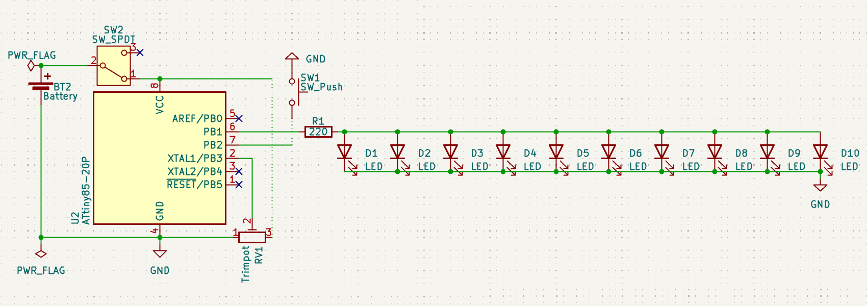
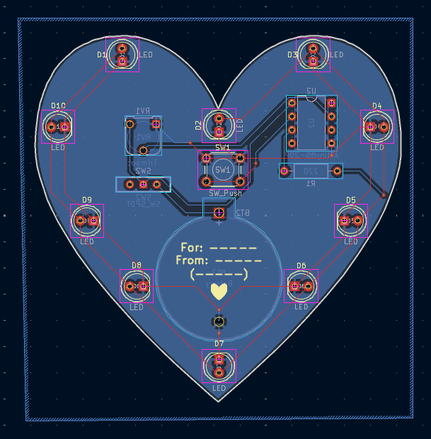
The full bill of materials with links and USD prices is in BOM.csv
Check it out in action:
| Qty | Value | Footprint | References |
|---|---|---|---|
| 10 | LED | LED_THT:LED_D5.0mm | D1, D2, D3, D4, D5, D6, D7, D8, D9, D10 |
| 1 | 220 | Resistor_THT:R_Axial_DIN0207_L6.3mm_D2.5mm_P10.16mm_Horizontal | R1 |
| 1 | ATtiny85-20P | Package_DIP:DIP-8_W7.62mm | U2 |
| 1 | Battery | Battery:BatteryHolder_MYOUNG_BS-07-A1BJ001_CR2032 | BT2 |
| 1 | SW_Push | Button_Switch_THT:SW_PUSH_6mm | SW1 |
| 1 | SW_SPDT | Button_Switch_THT:SW_Slide-03_Wuerth-WS-SLTV_10x2.5x6.4_P2.54mm | SW2 |
| 1 | Trimpot | Potentiometer_THT:Potentiometer_Runtron_RM-065_Vertical | RV1 |
bwack/C64-Switchless-Multi-Kernal-27C256-adapter
Kernal switcher for the C64/C64C/C128

plusvic/simplebus2-intercom
General description of the Simplebus2 protocol used by some Comelit's intercoms. Hardware for retransmitting Simplebus2 messages over UART.

osmocom/osmocom-analog
Software Implementation of analog cellular telephony systems like NMT, TACS, IMTS, A/B/C-Netz; mirror of https://gitea.osmocom.org/cellular-infrastructure/osmocom-analog

strickyak/jerboa-attiny85-mod-synth
Modular Synthesizer using an ATtiny85 chip for each module.


Hack-a-Day/Remoticon_KiCad_Blender
support files for the 2020 Remoticon KiCad to Blender > PCB renders workshop

It measures 70 × 70 mm and has 2 copper layers, 1.6 mm thick.
16 parts, built around the ATTINY85-20PU. The full list of its parts is on this page, with links to each part's symbol and footprint where PCBKit's library has them.
From the vindognz/project-luminescence repository on GitHub, at the commit this page was made from: the board is pcb/kicad.kicad_pcb and its schematic pcb/kicad.kicad_sch. PCBKit opens the board in the browser, with nothing to install.
Its repository states no licence, so its author keeps all rights: ask vindognz before reusing the design.