Skip to the content
PCBKitNew board
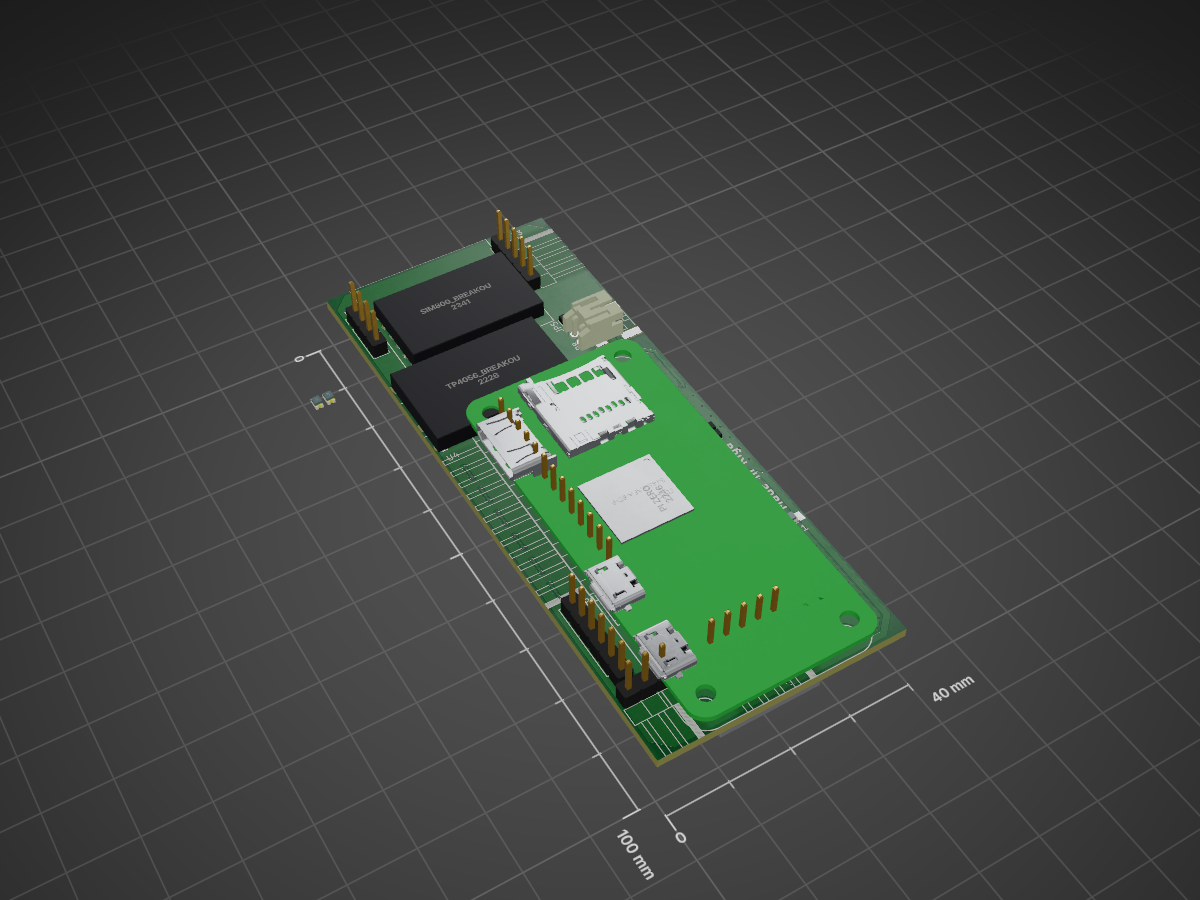
2 layers40 × 100 mmBack prototype, the printed circuit board in 3D

Back prototype

vgisc/ZeroPhone-PCBs1

This is gamma version. It's WIP and is going to be sent to production soon (as soon as last TODOs are finished). You can already order this board, but it's possible the I2C GPIO expander pin mapping is going to change.

Size
40 × 100 mm
Copper layers
2
Thickness
1.6 mm
Parts
68
Nets
53
Pads
255
Tracks, vias
561, 67
Pours
8
Routed
Yes
KiCad
KiCad 4
Created
28 Nov 2017
Updated
28 Nov 2017

Overview

Back prototype is an open-source printed circuit board by vgisc, from the vgisc/ZeroPhone-PCBs repository on GitHub, published under the GPL-3.0 licence. It is a 2-layer board of 40 × 100 mm with 68 parts on 53 nets, routed with 561 tracks and 67 vias.

It is built around the MCP23017-E/SS, IRLML6401 and SS14. Its parts include 21 capacitors, 9 resistors, 8 connectors, 5 ICs and 3 transistors. It belongs with the AVR (ATmega, ATtiny) boards of this library.

Main components

3

README

README.md

ZeroPhone-PCBs

KiCad PCB files for ZeroPhone

This is gamma version. It's WIP and is going to be sent to production soon (as soon as last TODOs are finished). You can already order this board, but it's possible the I2C GPIO expander pin mapping is going to change. Also, before ordering, please make sure the Gerber files are recent (if they're up-to-date after latest commits concerning PCB files) and regenerate them if necessary.

Features added, problems fixed - compared to beta version:

New things in "Gamma" front board:

  • Added 7-pin header for 1.3 SPI OLED display
  • Added trace closing the audio buffer override jumper
  • Lowered ATMega header pin count to 6 pins, one is selectable between ATMEGA_RST and ATMEGA_GPIO
  • Added a capacitor in series with ATMEGA_RST pin (for easier programming using off-the-shelf adapters)
  • Added a LED to ATMega PB5 (Arduino Pin 13) - optional, useful mostly for debugging
  • Added fiducials
  • Moved traces to get a ground plane between I2C and SPI, as well as between SPI MOSI and SPI CLK
  • Moved GSM audio filtering capacitors near mic to other layer
  • Changed all 0603 footprints to handsoldering ones
  • Fixed audio jack silkscreen so that it's shown correctly at the back of the board
  • Added a hole for GSM speaker wires to go through
  • Adjusted traces to account for soldermask tolerances
  • Replaced 10uF with 100uF capacitors on schematic
  • On display headers, changed middle pin drills to be smaller (for easier soldering of displays)
  • Added place for audio-to-ground resistors (like on Pi 3)
  • Bigger holes in pin headers
  • Changed the pins for the new revision - freeing up I2S/SPI1 interface
  • Shifted ESP-12 a tad further into board outline
  • Added revision info text, MakeRiga reference, OSHW and hacker glider labels
  • Added basic audio jack ESD protection
  • Modified audio jack output capacitor footprint so that 1206 would kinda fit
  • Fixed audio jack footprint
  • Adjusted GSM header pinout - to be in sync with back board
  • Added a GSM speaker cutout, moved its testpoints
  • Added a cutout where the ESP-12 antenna is
  • Adjusted ATMega's crystal's ground restrict polygon
  • Moved fiducials so as to avoid silkscreen lines on them
  • Moved ESD diode and audio-to-ground resistors to front layer
  • Decreased ground fill clearances
  • Centered display header
  • Un-hardwired 7-pin display header

New things in "Gamma" back board:

  • Turned MCP23017 to 180 degrees, rearranged its GPIOs
  • Removed I2C level shifting
  • Powered MCP23017 and RGB LED from VBAT
  • Added one more USB port
  • Fixed expansion header silkscreen
  • Swapped lots of pins on expansion headers - for easier routing
  • One layer for ground&power, one for signals
  • Changed all 0603 footprints to handsoldering ones
  • Adjusted GSM header pinout for easier routing - in sync with front board
  • Fixed footprint holes where they'd be too tight for pin headers
  • Added fiducials
  • Added OSHW logo, release information
  • Added a VSYS capacitor
  • Added a capacitor in parallel with the battery
  • Removed the MCP_INT testpoint and testpoints for free MCP GPIOs
  • Remove the footprint for additional protection IC
  • Added a footprint for MPU9050/9150 breakouts
  • Added a FET that interrupts VBAT+ and is controlled from GPIO expander (with a button to reset it?)
  • Adjusted protection footprint for protection boards I have (dirty hack, ugly and I hate it, maybe I should order another boards)

Parts

68
QtyValueFootprintReferences
10TEST_1PMeasurement_Points:Measurement_Point_Square-SMD-Pad_SmallW1, W2, W3, W4, W9, W10, W13, W25, W26, W29
9100nFCapacitors_SMD:C_0805_HandSolderingC1, C2, C5, C6, C8, C13, C14, C15, C25
610KResistors_SMD:R_0805_HandSolderingR1, R2, R3, R4, R10, R11
610pFCapacitors_SMD:C_0603_HandSolderingC16, C17, C18, C19, C20, C21
3100uFCapacitors_Tantalum_SMD:CP_Tantalum_Case-B_EIA-3528-21_HandC3, C4, C7
31KResistors_SMD:R_0805_HandSolderingR5, R6, R7
333pFCapacitors_SMD:C_0603_HandSolderingC22, C23, C24
3IRLML6401TO_SOT_Packages_SMD:SOT-23_HandsolderingQ1, Q2, Q4
2JUMPERConnect:GS2JP1, JP5
2JUMPERcommon-footprints:GS2_SMALLJP11, JP12
1A0common-footprints:GS3_SMALLJP3
1A1common-footprints:GS3_SMALLJP4
1A2common-footprints:GS3_SMALLJP6
1ATMEGA_HEADERPin_Headers:Pin_Header_Straight_1x06_Pitch2.54mmP6
1ATMEGA_VCCMeasurement_Points:Measurement_Point_Square-SMD-Pad_SmallW27
1AUDIO_CONNPin_Headers:Pin_Header_Straight_1x04_Pitch2.54mmP5
1DC_DC_BREAKOUTfootprints:DC-DC-BREAKOUTU6
1EXPANSION_BOTTOMPin_Headers:Pin_Header_Angled_1x05_Pitch2.54mmP2
1EXPANSION_BOTTOM2Pin_Headers:Pin_Header_Angled_1x03_Pitch2.54mmP7
1EXPANSION_LEFTPin_Headers:Pin_Header_Angled_1x13_Pitch2.54mmP1
1EXPANSION_TOPPin_Headers:Pin_Header_Angled_1x05_Pitch2.54mmP3
1GNDMeasurement_Points:Measurement_Point_Square-SMD-Pad_SmallW6
1JSTfootprints:JST_PH_S2B-PH-SM4-TB_02x2.00mm_AngledP8
1Led_RGB_CA_CCfootprints:RGB_5050D3
1MCP23017Housings_SOIC:SOIC-28W_7.5x17.9mm_Pitch1.27mmU3
1PI ZEROcommon-footprints:pi0outlineU1
1SIM800_BREAKOUTfootprints:SIM800_BREAKOUTU2
1SS14Diodes_SMD:D_MiniMELF_HandsolderingD1
1SW_PUSHfootprints:SW_SPST_EVQPE1SW1
1TP4056_BREAKOUTfootprints:TP4056_BREAKOUTU4
1USB_Afootprints:USB_AP9

Questions

How big is the Back prototype PCB?

It measures 40 × 100 mm and has 2 copper layers, 1.6 mm thick.

What parts does the Back prototype use?

68 parts, built around the MCP23017-E/SS, IRLML6401 and SS14. The full list of its parts is on this page, with links to each part's symbol and footprint where PCBKit's library has them.

Where can I download the Back prototype KiCad files?

From the vgisc/ZeroPhone-PCBs repository on GitHub, at the commit this page was made from: the board is back_pcb/back_prototype.kicad_pcb. PCBKit opens the board in the browser, with nothing to install.

Can I use the Back prototype design in my own project?

Its repository publishes it under the GPL-3.0 licence: you may reuse it on that licence's terms (keep the author's notice, and for a copyleft licence share your changes alike).

More from vgisc/ZeroPhone-PCBs

1
  • 2 layers40 × 100 mmFront prototype, the printed circuit board in 3D

    Front prototype

    vgisc/ZeroPhone-PCBs

    This is gamma version. It's WIP and is going to be sent to production soon (as soon as last TODOs are finished). You can already order this board, but it's possible the I2C GPIO expander pin mapping is going to change.

    87 parts1GPL-3.0

Similar boards

  • 2 layers40 × 100 mmBack pcb, the printed circuit board in 3D

    Back pcb

    ZeroPhone/ZeroPhone-PCBs

    PCB files for ZeroPhone - for gerbers and schematics, go to "Releases" tab!

    118 parts148GPL-3.0
  • 2 layers40 × 100 mmBack prototype, the printed circuit board in 3D

    Back prototype

    libresmartphone/libresmartphone

    This page contains the software used in the open hardware smartphone (libresmartphone)

    86 parts33
  • 2 layers87 × 79 mmZero node kicad, the printed circuit board in 3D

    Zero node kicad

    so1der/zero-node

    Standalone Meshtastic repeater based on the RP2040 Zero

    39 parts28
  • 2 layers29.8 × 49.8 mmGummySlime, the printed circuit board in 3D

    GummySlime

    gumorr/GummySlime

    Cheesecake compatible SlimeVR pcbs

    28 parts1
  • 2 layers42.8 × 88 mm18650 pcb, the printed circuit board in 3D

    18650 pcb

    CRImier/MyKiCad

    My KiCad boards. Can't be bothered uploading individually anymore, so here you go.

    48 parts253GPL-3.0
  • 2 layers129.5 × 50.8 mmLilka, the printed circuit board in 3D

    Lilka

    lilka-dev/lilka

    Схема та документація ігрової консолі Lilka

    39 parts234GPL-2.0
  • 4 layers41.4 × 108 mmM17 3310, the printed circuit board in 3D

    M17 3310

    M17-Project/M17_3310

    Mainboard replacement for Nokia 3310

    124 parts68