2 layers40 × 100 mm
Back pcb
ZeroPhone/ZeroPhone-PCBs
PCB files for ZeroPhone - for gerbers and schematics, go to "Releases" tab!
118 parts148GPL-3.0
 so1der/zero-node28
Standalone Meshtastic repeater based on the RP2040 Zero
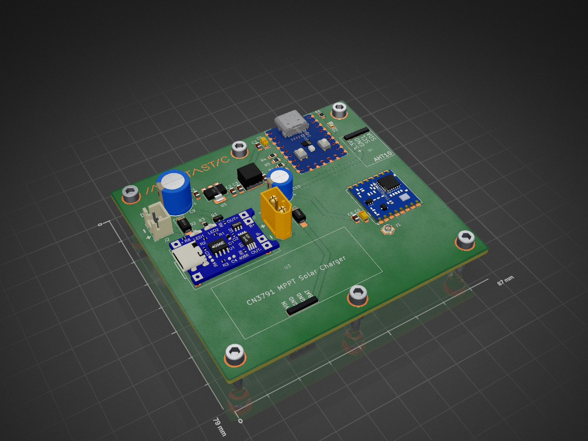
Zero node kicad is an open-source printed circuit board by so1der, from the so1der/zero-node repository on GitHub. It is a 2-layer board of 87 × 79 mm with 39 parts on 36 nets, routed with 115 tracks and 33 vias.
It is built around the RP2040-ZERO, SS14 and IRLML6401. Its parts include 10 capacitors, 6 resistors, 6 ICs, 3 diodes and 3 connectors. It belongs with the radio and wireless and power boards and the RP2040 boards of this library.


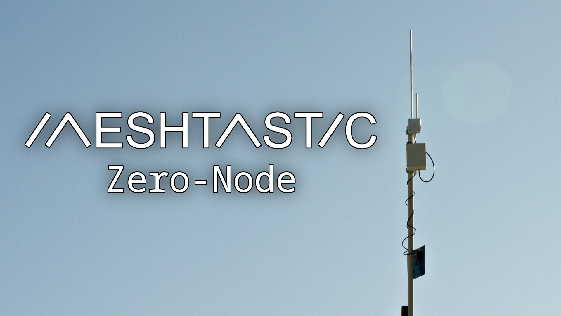
Zero Node is a standalone Meshtastic repeater based on the RP2040 Zero microcontroller and the Ra-01/Ra-02 radio modules. It has a CN3791 module for charging from the solar panels, as well as a TP4056 for charging from an external power supply if one is provided. The low consumption of the repeater (~20 mA in idle mode) will ensure operation for 100-250 hours with a 6000 mAh battery without any recharging. With a small solar panel, the operating time increases radically - a 3 W solar panel can almost completely compensate for the repeater's consumption even on winter sunless days. Paired with a good, high-mounted antenna, this repeater will be an excellent solution for expanding the coverage of your Meshtastic network!
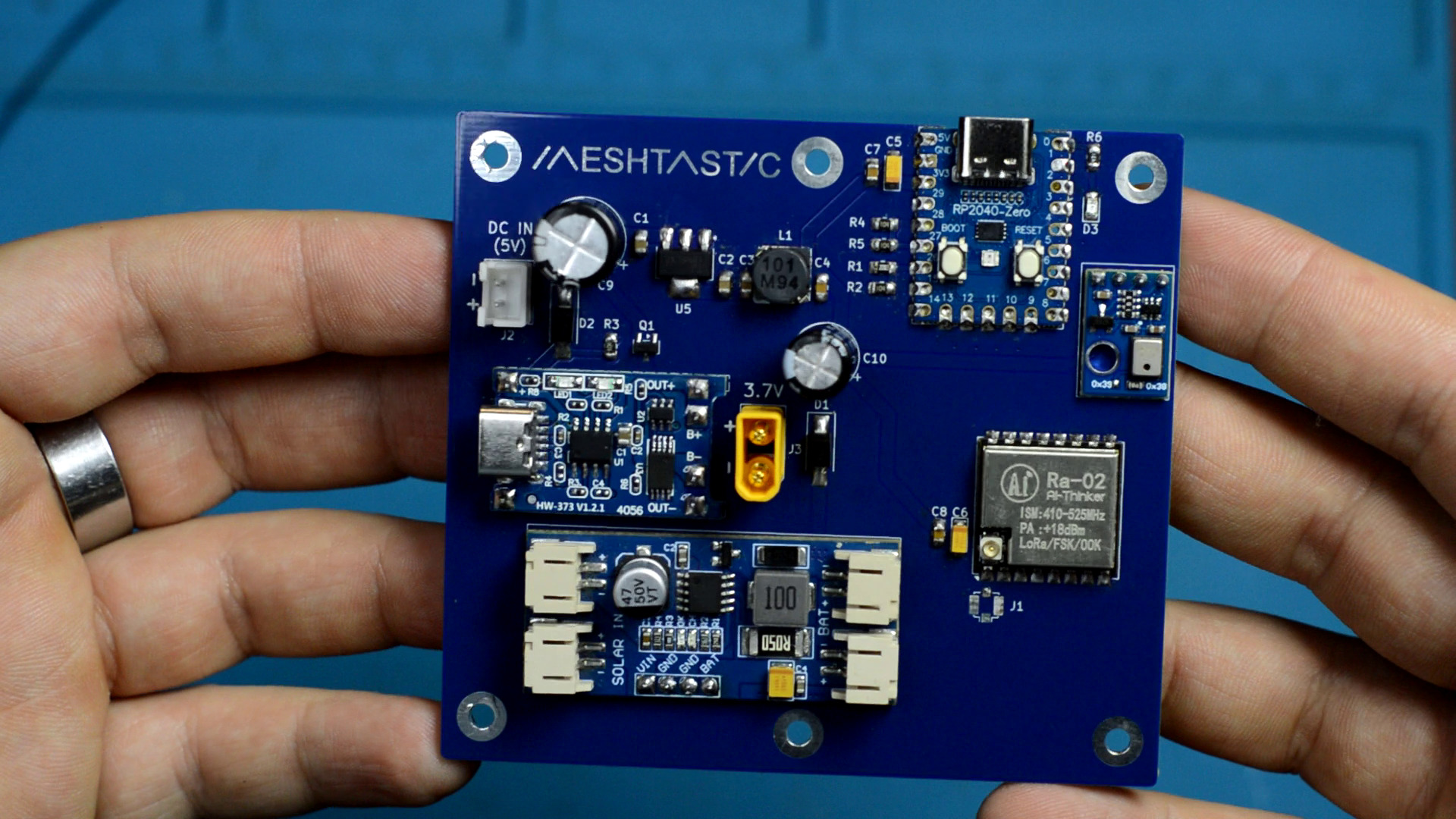
In order to flash the RP2040 microcontroller, it is enough to simply hold down the BOOT button on the microcontroller, and then connect it to the computer. The microcontroller will connect as a flash drive, to which you need to drop a special .uf2 file. .uf2 files with the firmware for this repeater are provided in the "firmware" directory of this git repository. There are two firmwares types - fast-cpu and slow-cpu. When each of them is needed is described in the next section.
By default, the microcontroller consumes about 40 mA of current on the 3.3V line. We can reduce this consumption by half by reducing the microcontroller clock frequency - from 133 MHz to 18 MHz. However, in this case, two problems arise - first, USB stops working (however, the microcontroller can still be flashed via USB), and therefore it is necessary to use an external UART converter to interact with the repeater (pins 0 - Tx, 1 - Rx). Secondly, personally, in my case, the repeater stops executing commands via UART - it receives them, responds, but does not execute them, so you cannot configure the repeater in this way. To get around this problem, you can first configure the node on the firmware with a normal clock frequency, and only after that upload the firmware with a reduced clock frequency - the settings are stored in the microcontroller's memory, so everything will work as it should.
Therefore, there are two firmware in the firmware folder:
It should also be noted that at 3.4V on the battery, the repeater will go into a deep sleep - Super Deep Sleep, so be sure to configure its duration. RP2040 does not know how to exit SDS, so it will simply reboot when time comes.
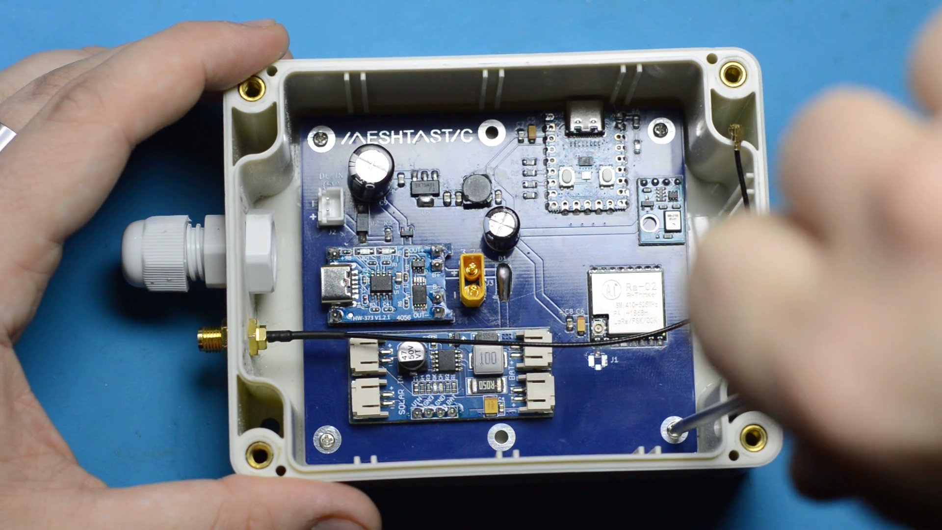
The repeater board should fit most moisture-proof cases measuring 115x90 mm. Personally, I used the case 11-3 from Sanhe. Judging by the drawings, the G311MF and G221CMF from Gainta should also fit. Below are links to the cases and their drawings:
To compile the firmware for this repeater, I created a separate variant file and also slightly modified the Meshtastic code. Since the changes are not very significant, I did not create a separate fork of the Meshtastic repository, but instead made a git patch. So to compile the firmware you need to clone the Meshtastic repo, open it, download my patch, and apply it:
git clone https://github.com/meshtastic/firmware
cd firmware
wget https://raw.githubusercontent.com/so1der/zero-node/refs/heads/main/zero-node.patch
git apply -v zero-node.patch
After that, the firmware can be compiled in a way convenient for you - via VS Code + PlatformIO, or via PlatformIO Core. The patch added a new PlatformIO environment called zero-node, so before compiling you need to select it, either in the general platformio.ini file:
[platformio]
default_envs = zero-node
Or at the compilation stage using PlatformIO Core:
pio run -e zero-nodeAfter compiling, the .uf2 file will be available at the path firmware/.pio/build/zero-node/. You can manually "drag" it to the microcontroller, or you can directly in VS Code click the "Upload" checkbox (Ctrl + Alt + U), or run the command:
pio run -e zero-node --target uploadThe main board settings are made in a special variant.h file of the board at the path: variants/rp2040/zero-node/variant.h. By default, you compile the firmware with a normal clock speed. To compile the firmware with a reduced clock speed, uncomment the corresponding define at the beginning of the file.
Normal clock speed:
// Reduce clock speed down to 18 MHz to reduce power consumption
//#define RP2040_SLOW_CLOCK
Reduced clock speed:
// Reduce clock speed down to 18 MHz to reduce power consumption
#define RP2040_SLOW_CLOCK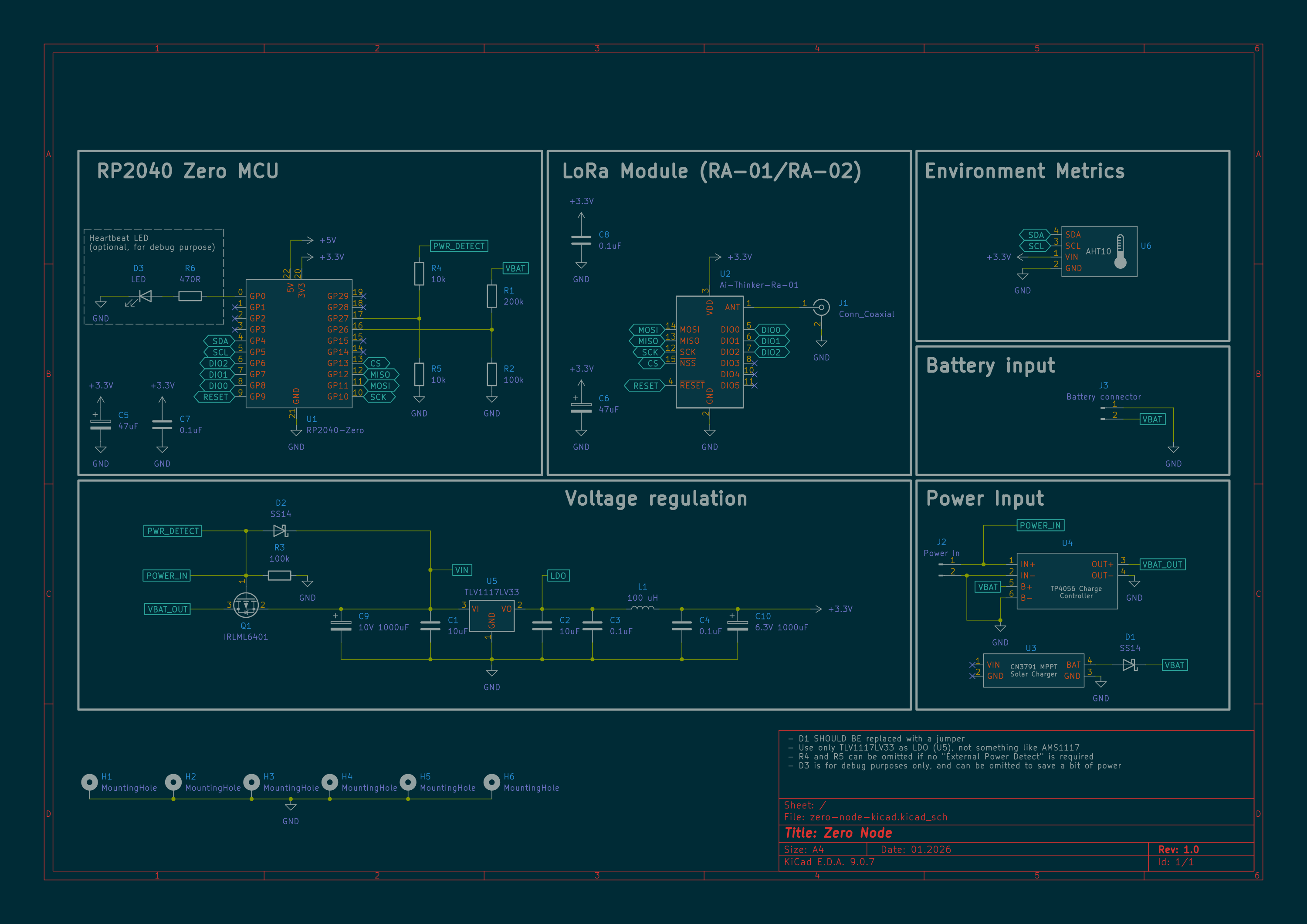
Key points regarding the schematic:
Zero Node - це автономний Meshtastic-ретранслятор, побудований на основі мікроконтролера RP2040 Zero, та радіомодулів Ra-01/Ra-02. Він має модуль CN3791 для зарядки від сонця, а також TP4056 для зарядки від зовнішнього блока живлення якщо такий передбачено. Низьке споживання ретранслятора (~20 мА в стані спокою) забезпечить роботу впродовж 100-250 годин з акумулятором ємністю 6000 мАг без будь якої підзарядки. За наявності невеличкої сонячної панелі час роботи радикально підвищується - сонячна панель на 3 Вт здатна майже повністю компенсувати споживання ретранслятора навіть в зимні безсонячні дні. В парі з гарною, високо розташованою антеною, даний ретранслятор стане чудовим рішенням для розширення покриття вашої Meshtastic мережі!
Для того щоб прошити мікроконтролер RP2040, достатньо всього лише затиснути кнопку BOOT на мікроконтролері, після чого підключити його до комп'ютера. Мікроконтролер підключиться у вигляді флеш накопичувача, на який треба скинути спеціальний .uf2 файл. .uf2 файли з прошивкою для даного ретранслятора знаходяться в директорії "firmware" даного гіт репозиторія. Там міститься два типи прошивки - fast-cpu та slow-cpu. Навіщо потрібна кожна з них - описано в наступному розділі.
За замовчуванням мікроконтролер споживає близько 40 мА струму по 3.3V лінії. Ми маємо змогу зменшити це споживання вдвічі, зменшивши тактову частоту мікроконтролера - з 133 МГц до 18 МГц. Однак в такому випадку випливає дві проблеми - по перше, перестає працювати USB (однак мікроконтролер все ще можна прошити по USB), а отже треба використовувати зовнішній UART перетворювач для взаємодії з ретранслятором (піни 0 - Tx, 1 - Rx). По друге - особисто в мене ретранслятор в такому випадку перестає виконувати команди по UART - він їх приймає, відповідає, але не виконує, тому ретранслятор таким чином не налаштуєш. Щоб обійти дану проблему, можна спочатку налаштувати вузол на прошивці з звичайною тактовою частотою, і вже після цього залити прошивку з зниженою тактовою частотою - налаштування зберігаються в пам'яті мікроконтролера, тому все працюватиме як слід.
Тому в директорії firmware присутні дві прошивки:
Також слід зауважити, що при 3.4V на акумуляторі, ретранслятор піде в глибокий сон - Super Deep Sleep, тому обов'язково налаштуйте його тривалість. RP2040 не вміє виходити з SDS, тому він просто перезавантажиться.
Плата ретранслятора повинна підійти для більшості вологозахищених корпусів розміром 115х90 мм. Особисто я використав корпус 11-3 від Sanhe. Якщо судити по кресленням, то повинні підійти ще G311MF та G221CMF від Gainta. Нижче наведені посилання на корпуси та їх креслення:
Для компіляції прошивки для даного ретранслятора я створював окремий variant файл, а також трохи модифікував код Meshtastic. Через те, що зміни не дуже значні, я не створював окремий форк репозиторія Meshtastic, а натомість зробив git патч. Тож для компіляції прошивки треба клонувати репо Meshtastic, відкрити його, завантажити мій патч, та застосувати його:
git clone https://github.com/meshtastic/firmware
cd firmware
wget https://raw.githubusercontent.com/so1der/zero-node/refs/heads/main/zero-node.patch
git apply -v zero-node.patch
Після цього прошивку можна буде компілювати зручним для вас способом - через VS Code + PlatformIO, або виключно через PlatformIO Core. Патч додав новий PlatformIO environment під назвою zero-node, відповідно перед компіляцією треба обрати його, або в загальному platformio.ini файлі:
[platformio]
default_envs = zero-node
Або на етапі компіляції за допомогою PlatformIO Core:
pio run -e zero-nodeПісля компіляції .uf2 файл буде доступний за шляхом firmware/.pio/build/zero-node/. Можна вручну "перетягнути" його на мікроконтролер, або можна прямо в VS Code натиснути галочку "Upload" (Ctrl + Alt + U), чи виконати команду:
pio run -e zero-node --target uploadОсновні налаштування плати відбуваються в спеціальному variant.h файлі плати за шляхом: variants/rp2040/zero-node/variant.h. За замовчуванням ви скомпілюєте прошивку зі звичайною тактовою частотою. Щоб скомпілювати прошивку зі зменшеною тактовою частотою, розкоментуйте відповідний дефайн на початку файла.
Звичайна тактова частота:
// Reduce clock speed down to 18 MHz to reduce power consumption
//#define RP2040_SLOW_CLOCK
Зменшена тактова частота:
// Reduce clock speed down to 18 MHz to reduce power consumption
#define RP2040_SLOW_CLOCK
Основні моменти стосовно схеми:
| Qty | Value | Footprint | References |
|---|---|---|---|
| 6 | MountingHole | MountingHole:MountingHole_3mm_Pad | H1, H2, H3, H4, H5, H6 |
| 4 | 0.1uF | Capacitor_SMD:C_0805_2012Metric_Pad1.18x1.45mm_HandSolder | C3, C4, C7, C8 |
| 4 | 100k | Resistor_SMD:R_0805_2012Metric_Pad1.20x1.40mm_HandSolder | R2, R3, R4, R5 |
| 3 | LOGO | LOGO | G***, G***, G*** |
| 2 | 10uF | Capacitor_SMD:C_0805_2012Metric_Pad1.18x1.45mm_HandSolder | C1, C2 |
| 2 | 47uF | Capacitor_Tantalum_SMD:CP_EIA-3216-18_Kemet-A_HandSolder | C5, C6 |
| 2 | SS14 | Diode_SMD:D_SMA_Handsoldering | D1, D2 |
| 1 | 100 uH | Inductor_SMD:L_Cenker_CKCS6045 | L1 |
| 1 | 10V 1000uF | Capacitor_THT:CP_Radial_D10.0mm_P5.00mm | C9 |
| 1 | 200k | Resistor_SMD:R_0805_2012Metric_Pad1.20x1.40mm_HandSolder | R1 |
| 1 | 470R | Resistor_SMD:R_0805_2012Metric_Pad1.20x1.40mm_HandSolder | R6 |
| 1 | 6.3V 1000uF | Capacitor_THT:CP_Radial_D8.0mm_P3.50mm | C10 |
| 1 | Ai-Thinker-Ra-01 | RF_Module:Ai-Thinker-Ra-01-LoRa | U2 |
| 1 | Battery connector | Connector_AMASS:AMASS_XT30U-M_1x02_P5.0mm_Vertical | J3 |
| 1 | Conn_Coaxial | Connector_Coaxial:U.FL_Molex_MCRF_73412-0110_Vertical | J1 |
| 1 | IRLML6401 | Package_TO_SOT_SMD:SOT-23 | Q1 |
| 1 | LED | LED_SMD:LED_0805_2012Metric_Pad1.15x1.40mm_HandSolder | D3 |
| 1 | Power In | Connector_JST:JST_XH_B2B-XH-A_1x02_P2.50mm_Vertical | J2 |
| 1 | RP2040-Zero | footprints:RP2040-Zero | U1 |
| 1 | TLV1117LV33 | Package_TO_SOT_SMD:SOT-223-3_TabPin2 | U5 |
| 1 | ~ | footprints:Charge_Controller_TP4056_4pin | U4 |
| 1 | ~ | footprints:AHT10 | U6 |
| 1 | ~ | footprints:CN3791 MPPT Solar Charger | U3 |
It measures 87 × 79 mm and has 2 copper layers, 1.6 mm thick.
39 parts, built around the RP2040-ZERO, SS14 and IRLML6401. The full list of its parts is on this page, with links to each part's symbol and footprint where PCBKit's library has them.
From the so1der/zero-node repository on GitHub, at the commit this page was made from: the board is zero-node-kicad/zero-node-kicad.kicad_pcb and its schematic zero-node-kicad/zero-node-kicad.kicad_sch. PCBKit opens the board in the browser, with nothing to install.
Its repository states no licence, so its author keeps all rights: ask so1der before reusing the design.
ZeroPhone/ZeroPhone-PCBs
PCB files for ZeroPhone - for gerbers and schematics, go to "Releases" tab!


CRImier/MyKiCad
My KiCad boards. Can't be bothered uploading individually anymore, so here you go.

libresmartphone/libresmartphone
This page contains the software used in the open hardware smartphone (libresmartphone)

vgisc/ZeroPhone-PCBs
This is gamma version. It's WIP and is going to be sent to production soon (as soon as last TODOs are finished). You can already order this board, but it's possible the I2C GPIO expander pin mapping is going to change.

