4 layers49.3 × 53.8 mm
Novara main
abhisheknote1234-writ/Novara_PCB_Design
The HARDWARE design for the product - Intelligent maternal health monitoring using PPG for early detection of stress and pregnancy-related risks.
52 parts

 varaddorle007/deck-81
Open-source 8-key macro pad with 2 knobs, OLED and Bluetooth: PCB, case and ZMK firmware
Deck-8 is an open-source printed circuit board by varaddorle007, from the varaddorle007/deck-8 repository on GitHub, published under the MIT licence. It is a 4-layer board of 92.8 × 76 mm with 101 parts on 88 nets, routed with 1,037 tracks and 585 vias.
It is built around the SN74LV1T125DBV, MDBT50Q-1MV2 and BQ24074RGTR, with the TPS22917DBV, TPS7A0533PDBV and USBLC6-2SC6 among its other parts. Its parts include 27 capacitors, 20 resistors, 13 switches, 8 diodes and 7 ICs. It belongs with the keyboards and input boards and the nRF52 and nRF5x boards of this library.


An open-source 8-key macro pad with two knobs, a tiny screen and Bluetooth. Everything is in this repo: the circuit board, the 3D-printable case, the firmware, and every file you need to order the parts.
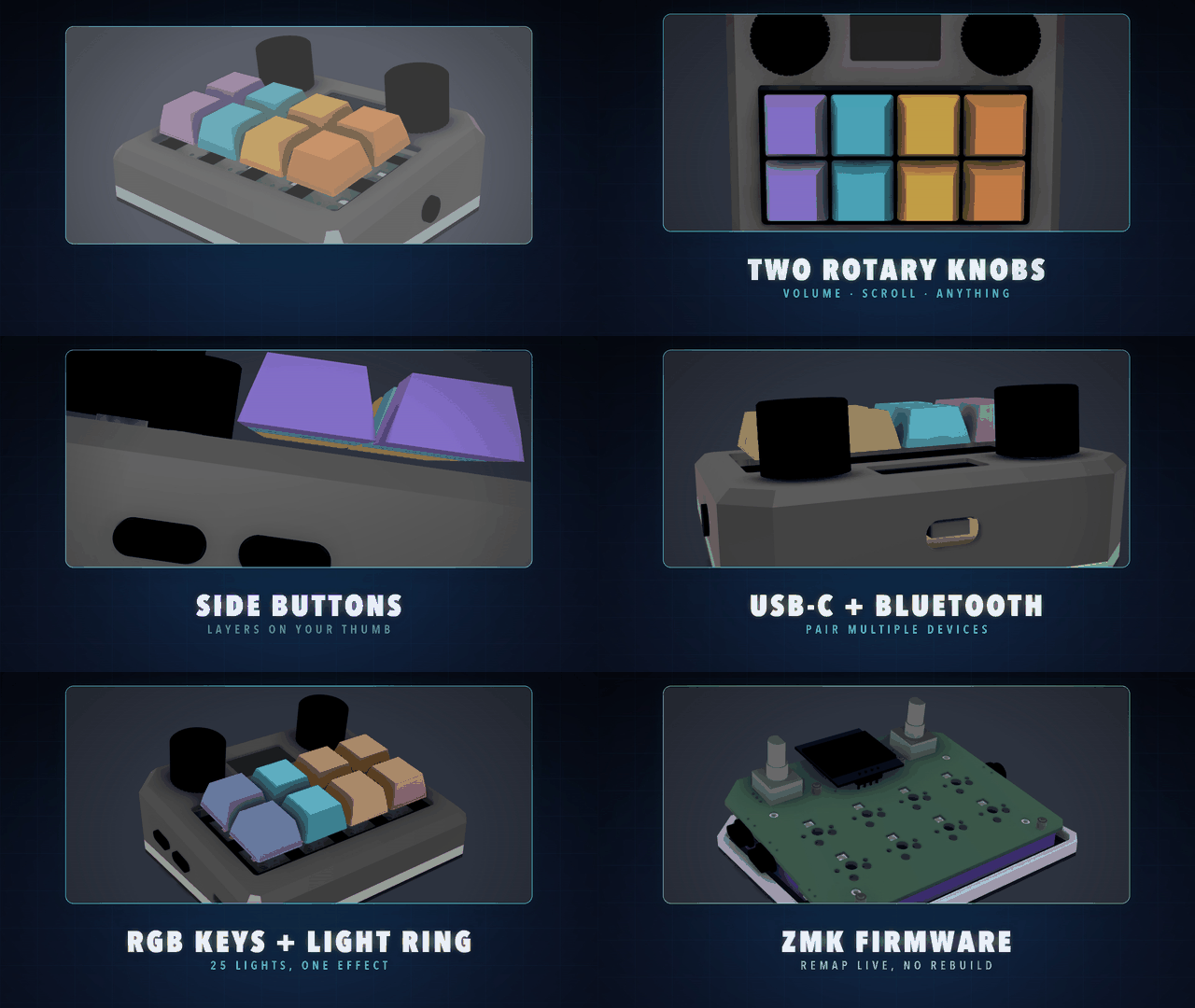
Click the preview for the full 30 second video with sound.
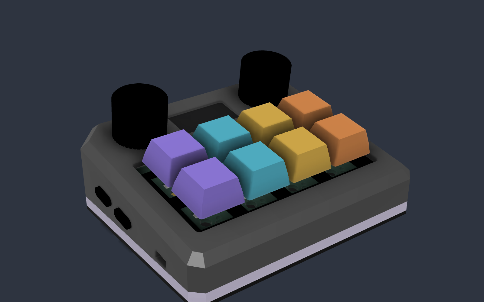
Status: Rev A, designed and checked, but not yet built. The board passes every automatic check (design rules, schematic checks, a fit check of the board in the case). The firmware compiles. But no one has built one yet, and the firmware has never run on real hardware. If you build one, you are the first. Please open an issue and tell us what happened, good or bad. See Known risks.
| Keys | 8 mechanical keys (MX-style, hot-swap, so you can change switches without soldering) in 2 rows of 4 |
| Knobs | 2 rotary knobs with push buttons (volume, scrolling, anything you map) |
| Screen | 0.96 inch OLED showing battery, connection and active layer |
| Side buttons | L1 and L2 on the left, System on the right, plus a power slide switch |
| Lights | RGB under every key, plus a glowing ring around the base |
| Connections | USB-C and Bluetooth (5 profiles) |
| Battery | Built-in 1000 mAh LiPo, charges over USB-C |
| Brain | Nordic nRF52840 (Raytac MDBT50Q module), running ZMK firmware |
| Remapping | Change keys live in ZMK Studio, no rebuild needed |
| Size | Case 98 × 84 mm, 18 mm tall at the front rising to 30 mm at the back (the top tilts 8°). Board 92.8 × 76 mm, 4 layers |
By default the 8 keys send F13–F20. No normal keyboard has those keys, so they never clash with anything. Bind them to anything you like in OBS, in your operating system, or in a Stream Deck-style app.
         [knob A]   [  OLED  ]   [knob B]
  [L1]   [ 1 ] [ 2 ] [ 3 ] [ 4 ]
[L2] [ 5 ] [ 6 ] [ 7 ] [ 8 ] [SYS]| Layer | How you get it | Keys 1–4 | Keys 5–8 | Knob A turn / press | Knob B turn / press |
|---|---|---|---|---|---|
| Bank 1 | default | F13 F14 F15 F16 | F17 F18 F19 F20 | volume / mute | ← → / play-pause |
| Media | hold L1 | prev, play/pause, next, mute | undo, redo, copy, paste | same | same |
| Bank 3 | hold L2 | Ctrl+F13–F16 | Ctrl+F17–F20 | same | same |
| System | hold SYS | Bluetooth profile 1–4 | clear profile, USB/Bluetooth, lights on/off, next effect | brightness / saturation | colour / unlock Studio |
On the System layer, L1 jumps to the bootloader (for updates) and L2 resets. Edit firmware/config/deck8.keymap to change any of this.
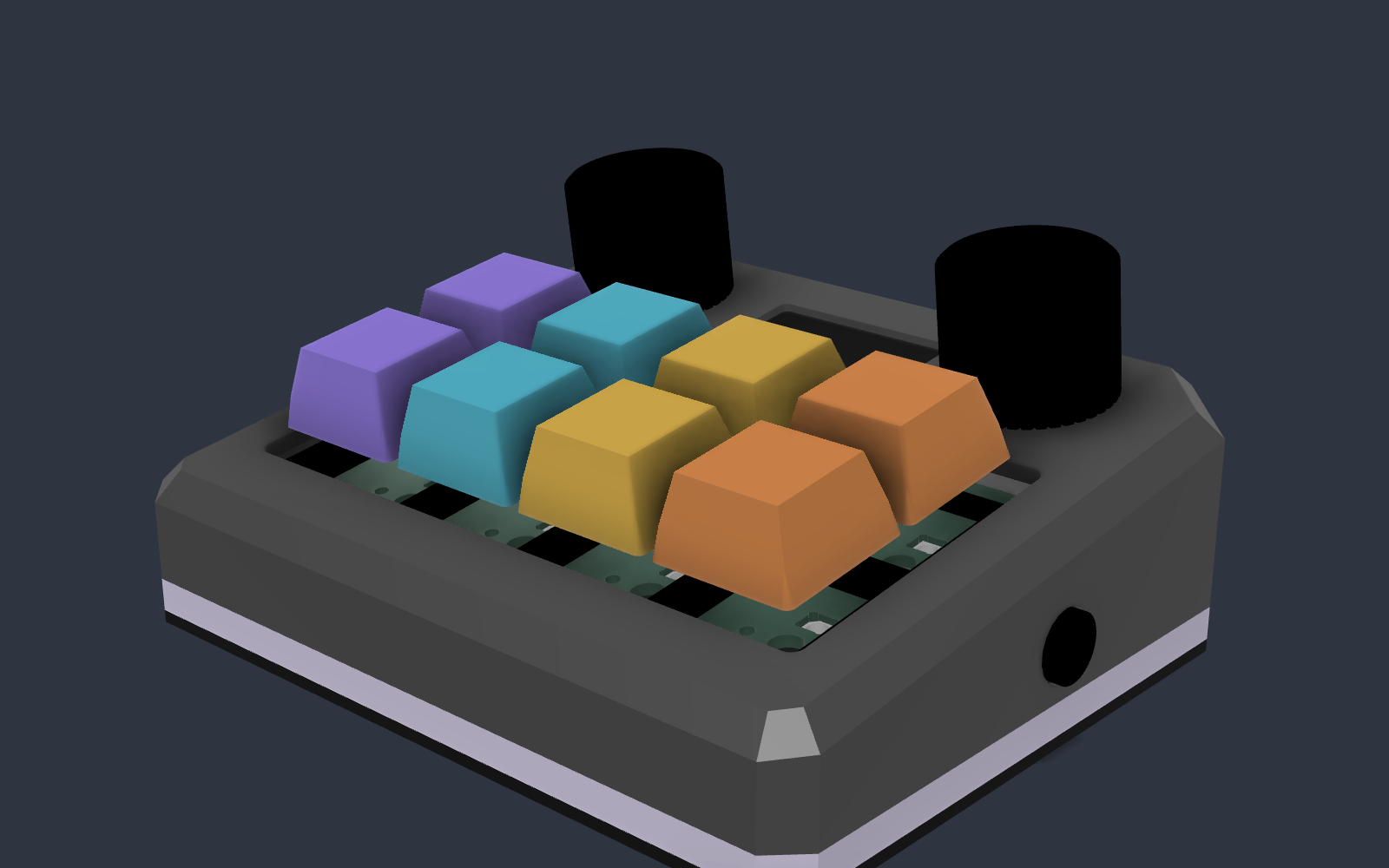 | 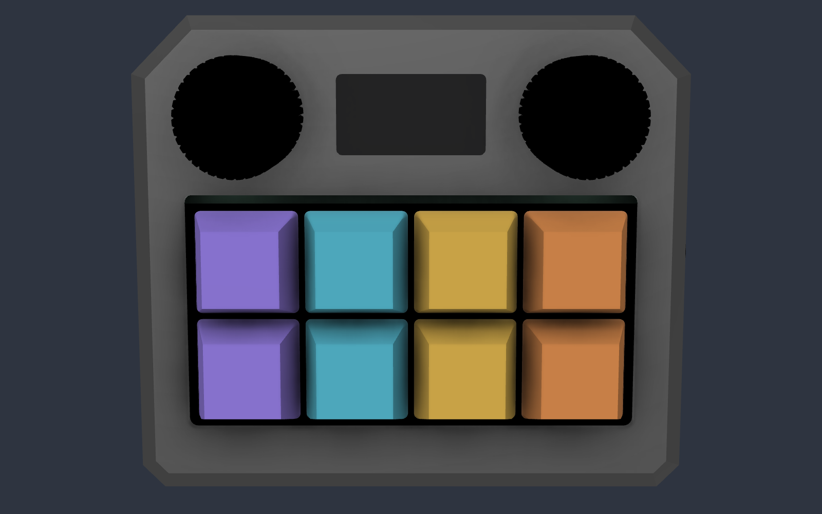 |
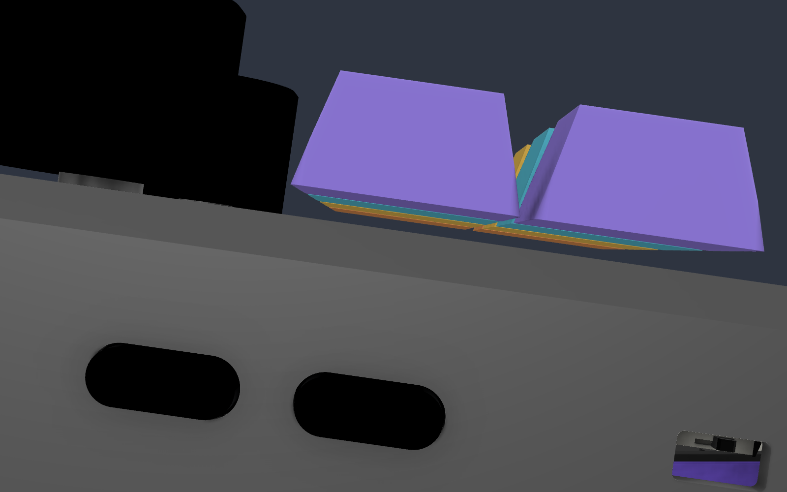 | 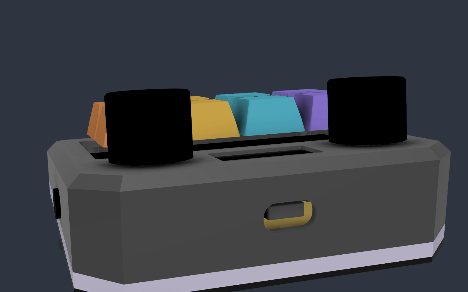 |
 | 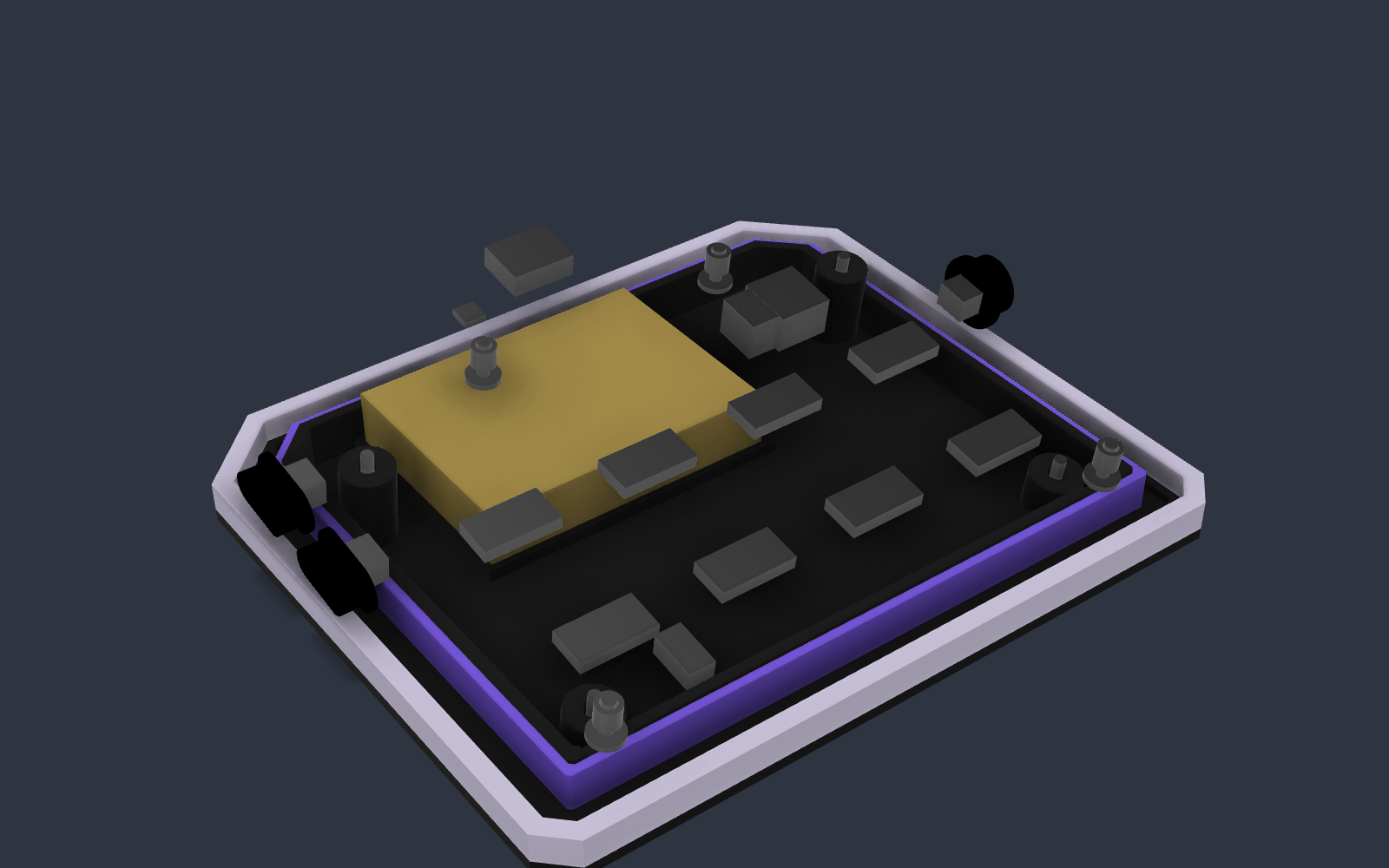 |
Bottom right: the tray, with the battery on the left and the glowing ring's wall around the edge. The 3D renders show the board and its parts as simple boxes where a part has no 3D model.
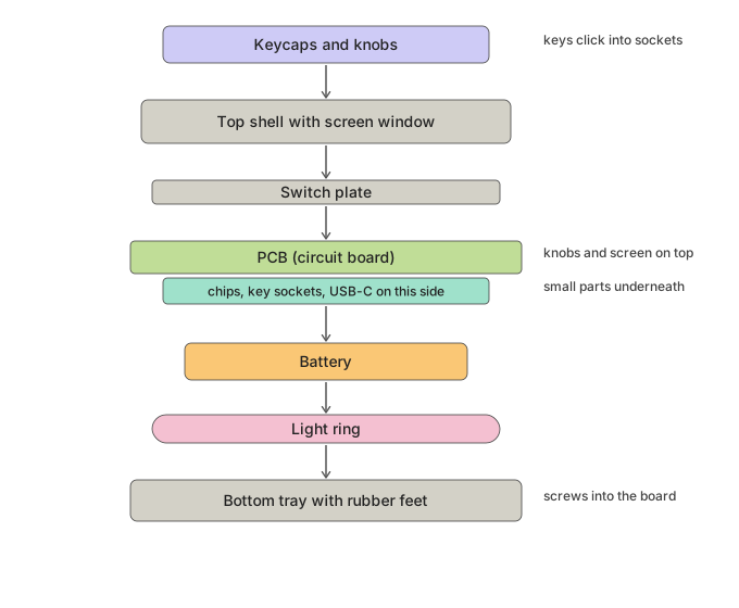
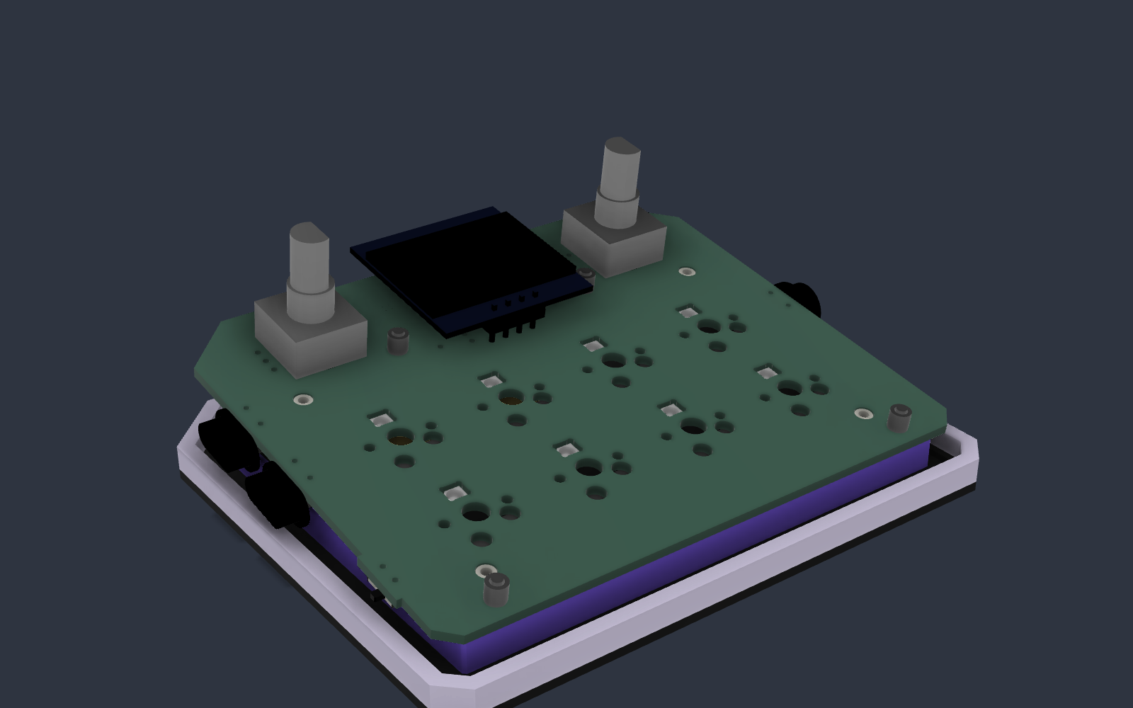
The board is a two-sided sandwich:
| Top | Bottom |
|---|---|
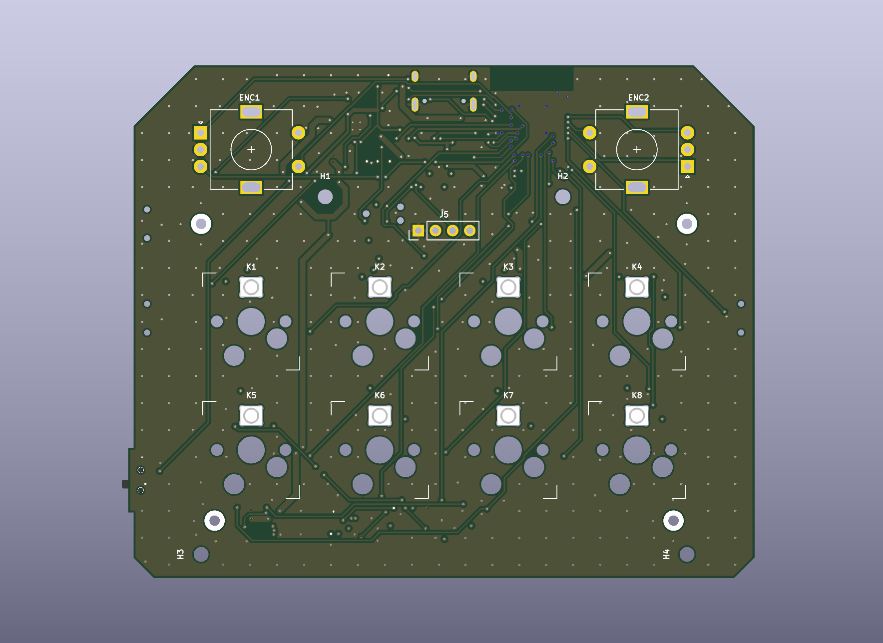 | 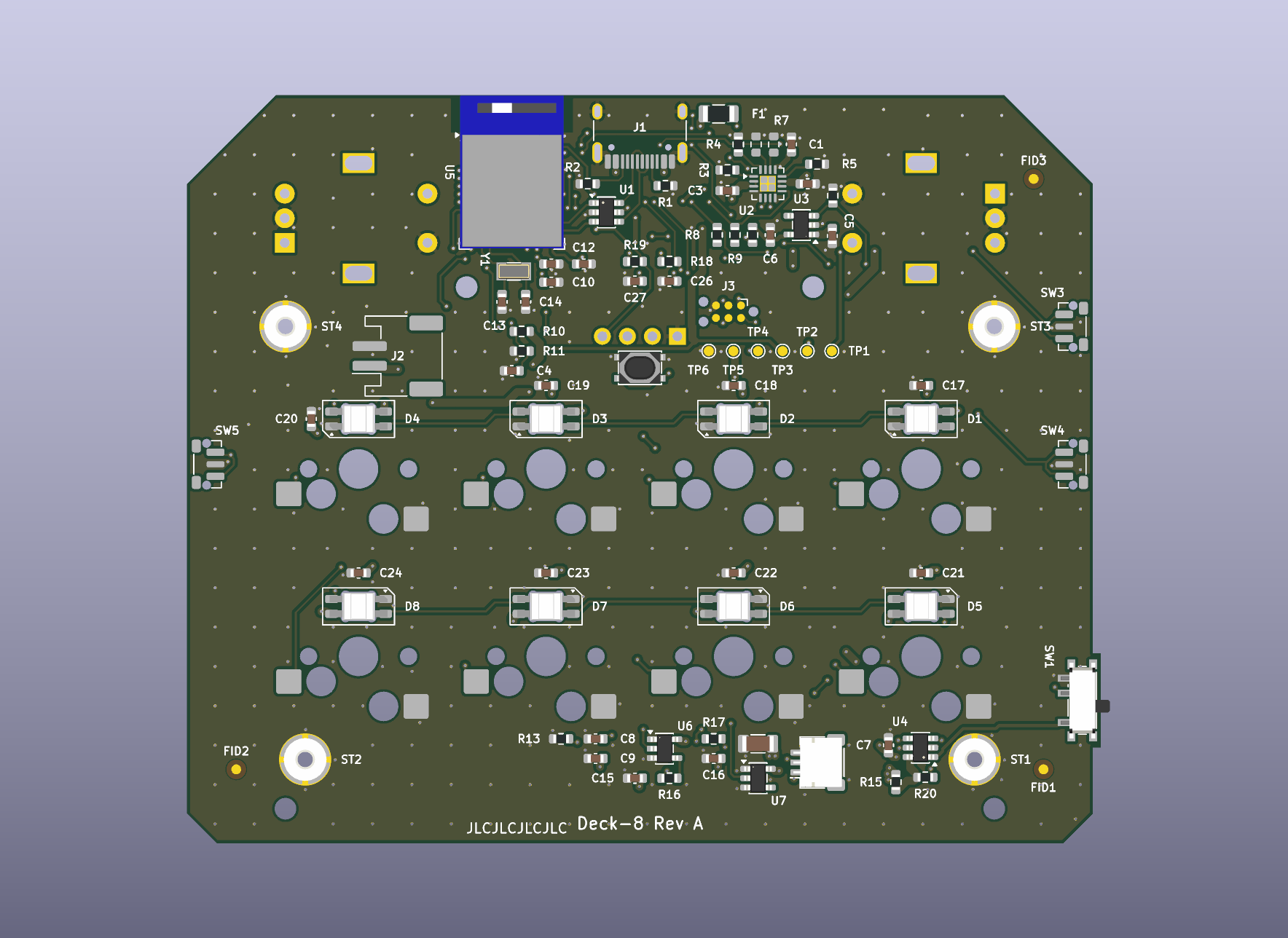 |
| 3D view, top | 3D view, bottom |
|---|---|
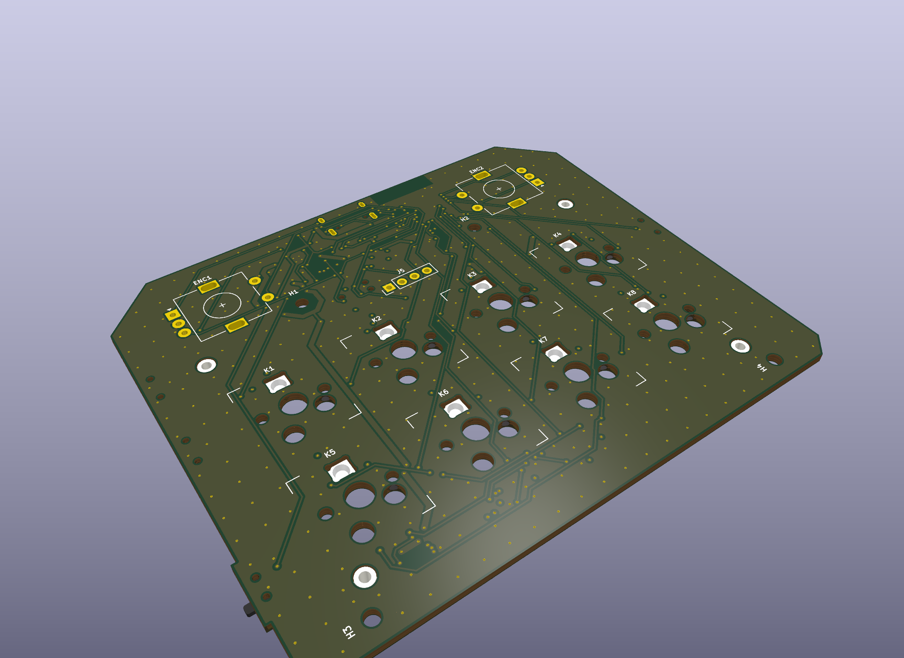 | 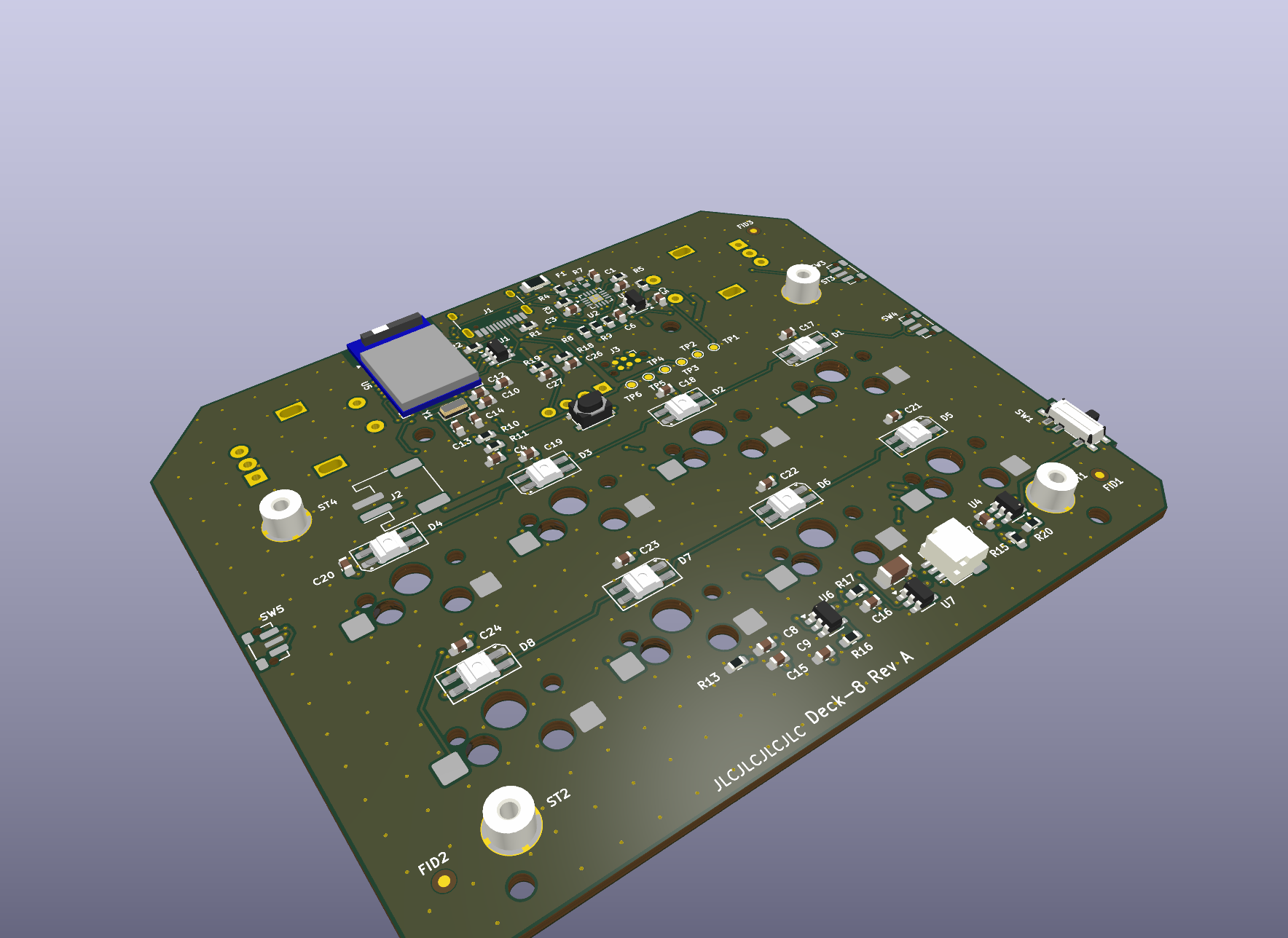 |
The PCB 3D views show the bare board; most parts have no 3D model in KiCad's library.
Four layers: top (signals), a full ground plane, a split power plane (3.3 V and the LED supply), and the bottom (parts and signals). 1037 tracks, 585 vias, USB data lines 14.5 and 15.2 mm long with no vias.
| Ground layer | Power layer |
|---|---|
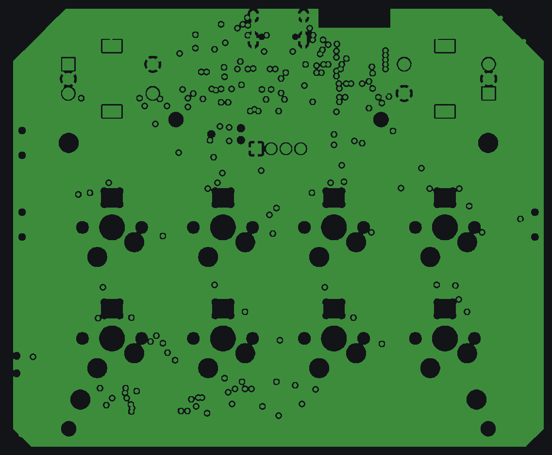 | 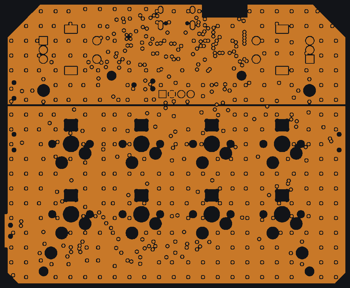 |
Seven sheets, all generated from hardware/tools/gen_schematic.py. The full set is in docs/deck8-schematic.pdf.
| Power: USB-C, charger, regulator, LED switch | MCU: nRF52840 and crystal |
|---|---|
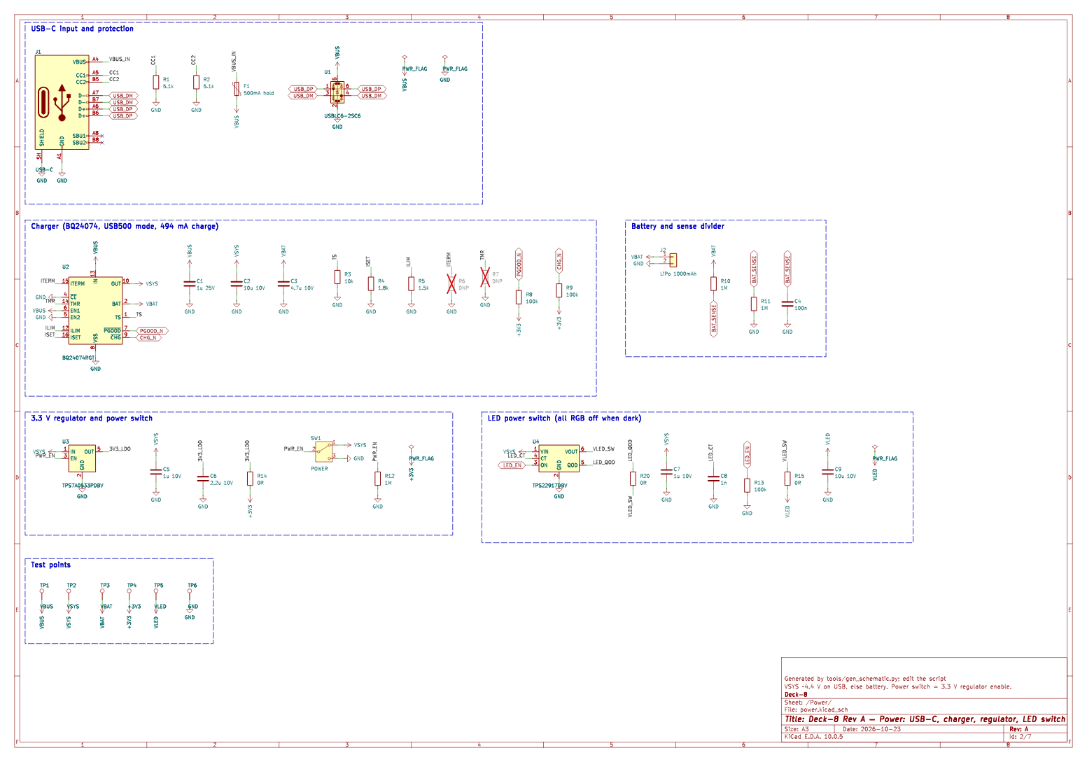 | 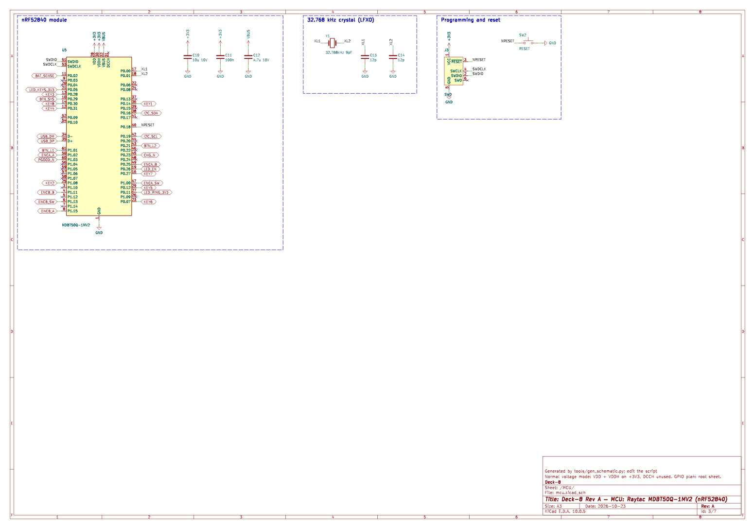 |
| Inputs: keys, buttons, knobs | Lighting | Display |
|---|---|---|
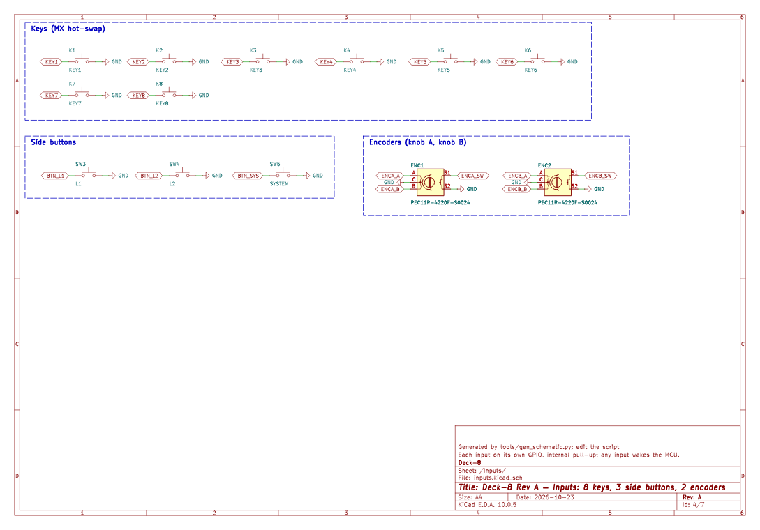 | 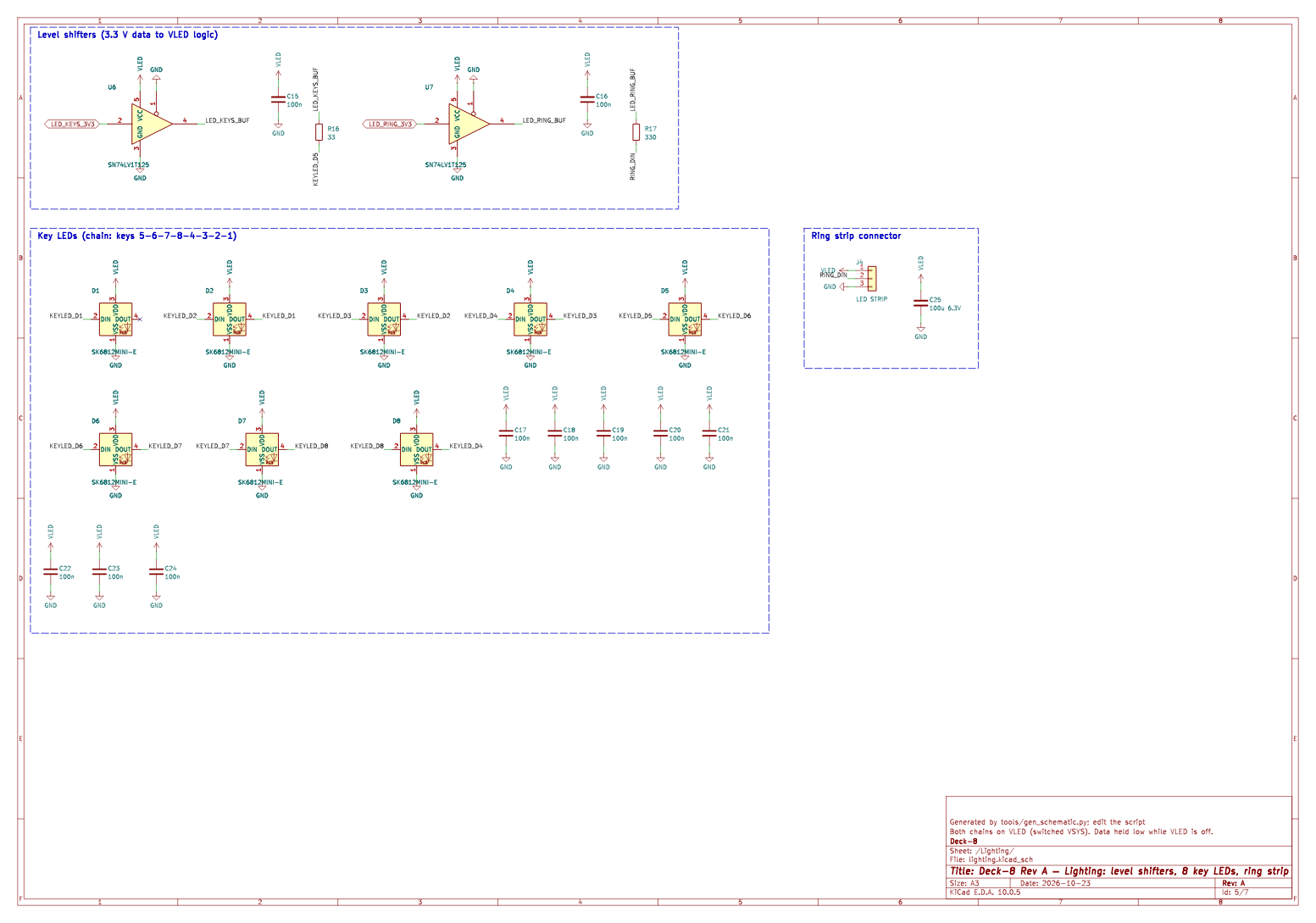 | 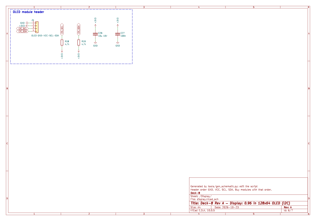 |
This is the plain version. release/BUILD-GUIDE.md has the same steps in more detail, and release/BUY-LIST.csv lists every part.
An honest estimate, from October 2026 prices. Check every number at the time you order:
| Item | Rough cost |
|---|---|
| Assembled boards from JLCPCB (3–5 boards, with all the small parts, setup fees and shipping) | about $150–200 total (₹13,000–17,000) |
| Parts you buy yourself: screen, 2 encoders, battery, LED strip, 8 switches, keycaps, screws | about $20–35 per unit |
| Printing the case | about $10–35, depending on where you print |
The big cost is not the board itself. A bare board is cheap (5 boards for about $8 with leaded HASL finish). The cost is assembly: setup fees, "extended part" fees, the parts, and shipping. If you can solder, you can order bare boards and build them, but the main chip's pads are underneath it (see the next section), so you will need a hot-air station.
The ready-to-upload files are in release/deck8-RevA-manufacturing/1-PCB-order-JLCPCB/:
| File | Upload it as |
|---|---|
deck8-RevA-gerbers.zip | The board design |
deck8-RevA-bom-jlc.csv | The parts list |
deck8-RevA-cpl-jlc.csv | Where each part goes |
Settings (all listed in JLC-ORDER-SETTINGS.md in the same folder): 4 layers, 1.6 mm thick, ENIG finish (HASL also works but is less flat), tented vias, assembly on the bottom side only, and "Confirm parts placement" turned on.
Watch for these on the JLCPCB parts page:
release/BUY-LIST.csv is the full list. Briefly:
Files are in release/deck8-RevA-manufacturing/3-Enclosure/. All STLs are in millimetres, laid flat.
| Part | Qty | Material |
|---|---|---|
| Top shell | 1 | MJF or SLS nylon (best), or FDM PETG/ASA. Nylon takes heat-set inserts. |
| Bottom tray | 1 | MJF nylon or FDM PETG |
| Light ring | 1 | Clear or translucent (clear SLA resin, sanded frosted). It must let light through. |
| Knob | 2 | MJF nylon or SLA (one file, print two) |
| Buttons (L1, L2, System) | 1 each | MJF nylon or SLA |
| Switch plate | 1 | Laser-cut 1.5 mm steel, aluminium or FR-4 from the DXF (best), or printed |
| OLED lens | 1 | 1 mm clear or smoked acrylic, laser-cut from the DXF |
The firmware is ready-built: release/deck8-RevA-manufacturing/4-Firmware/deck8.uf2.
Once per board (a new nRF52840 is empty): put the bootloader on through the Tag-Connect pads J3.
nice_nano_bootloader-0.11.0_s140_6.1.1.hex from the Adafruit bootloader releases. Its flash layout matches this board.nrfjprog --program nice_nano_bootloader-0.11.0_s140_6.1.1.hex --chiperase --verify --resetdeck8.uf2 onto it. The board restarts as "Deck-8".Updates: hold SYS and press L1, or double-press the RESET button (SW2), and copy the new .uf2 onto the drive.
First-power-up checks (the firmware has never run on real hardware, so check these):
segment-remap; and com-invdir; to the oled node in firmware/boards/deck8/deck8_nrf52840_zmk.dts. Blank? Delete inversion-on;.sensor-bindings in the keymap. Two steps per click? Set steps = <48> for that encoder.color-mapping or chain-length in the ring_leds node, and chain-length in all_leds (8 key LEDs + ring LEDs).See firmware/README.md for how the firmware is built and what each file does.
deck-8/
├── hardware/             the circuit board (KiCad 10)
│   ├── main/             the KiCad project: open deck8.kicad_pro
│   ├── lib/              the 4 custom footprints
│   ├── exports/          the board as a 3D STEP file (deck8_pcb.step)
│   ├── tools/            Python that generates, routes and checks the board and writes the fab files
│   └── README.md         how the board was designed, routed and checked
├── mechanical/           the case (Autodesk Fusion)
│   ├── fusion/Deck8Model/  script that builds the whole case; change a number and re-run
│   └── exports/          STEP, STL, renders and the clash-check report
├── firmware/             ZMK firmware: keymap, board definition, LED and battery code
├── release/              everything ready to upload, print and flash, plus the build guide and buy list
├── media/                the 30 second promo video
└── docs/                 images and the schematic PDF
Nothing is drawn by hand. The schematic, the board layout and the case are all produced by scripts, so a change is a few lines of code and a re-run. That also means edit the scripts, not the generated files.
You need macOS or edit the paths: the scripts point to KiCad at /Applications/KiCad/KiCad.app. You'll want KiCad 10, Python 3, Autodesk Fusion (the free personal or education licence works), and a C compiler for the router.
Board, from hardware/tools. KPY is KiCad's own Python, which includes pcbnew:
KPY=/Applications/KiCad/KiCad.app/Contents/Frameworks/Python.framework/Versions/Current/bin/python3
python3 gen_schematic.py && python3 check_schematic.py
$KPY gen_pcb.py && $KPY route_pcb.py && python3 check_pcb.py
$KPY make_fab.py
About a minute in total, with the same result every time. check_pcb.py runs KiCad's design-rule check and fails on anything. make_fab.py refuses to run unless the check passes, then writes the Gerbers, BOM and pick-and-place files and reads them all back to verify them.
The router is a small A* autorouter written for this project (hardware/tools/route_pcb.py plus a C core in hardware/tools/router/maze.c, compiled on first run).
Case, in Fusion: open Utilities → Add-Ins → Scripts and Add-Ins, add the folder mechanical/fusion/Deck8Model, and run it. It builds the case, loads the PCB from hardware/build/deck8_pcb.step, and writes the report and exports. If you copy the script into Fusion's own scripts folder instead, put the path of this repo in a file called deck8_root.txt next to it, or set the DECK8_ROOT environment variable. A clean build reports 0 errors and 0 clashes.
Firmware, from firmware/:
tools/setup_toolchain.sh   # once: about 4 GB into ~/zmk-build, nothing system-wide
tools/build.sh             # builds out/deck8.uf2
Release files: python3 release/tools/make_release.py collects the latest board, case and firmware files into release/deck8-RevA-manufacturing/.
Rev A is a first prototype. In order of how likely they are to bite:
firmware/boards/deck8/deck8_nrf52840_zmk_defconfig).Open an issue or a pull request.
MIT for the hardware design files, the case, the code and the docs. Do what you like with them, including selling them; please keep the licence notice. Third-party material is listed in NOTICE.md.
| Qty | Value | Footprint | References |
|---|---|---|---|
| 13 | 100n | Capacitor_SMD:C_0603_1608Metric | C4, C11, C15, C16, C17, C18, C19, C20, C21, C22, C23, C24, C27 |
| 8 | SK6812MINI-E | LED_SMD:LED_SK6812MINI-E_3.2x2.8mm_P1.5mm_ReverseMount | D1, D2, D3, D4, D5, D6, D7, D8 |
| 4 | 10u 10V | Capacitor_SMD:C_0603_1608Metric | C2, C9, C10, C26 |
| 4 | M2 boss | MountingHole:MountingHole_2.2mm_M2 | H1, H2, H3, H4 |
| 4 | M2x3 standoff | Mounting_Wuerth:Mounting_Wuerth_WA-SMSI-M2_H3mm_9774030243 | ST1, ST2, ST3, ST4 |
| 3 | 0R | Resistor_SMD:R_0603_1608Metric | R14, R15, R20 |
| 3 | 100k | Resistor_SMD:R_0603_1608Metric | R8, R9, R13 |
| 3 | 1M | Resistor_SMD:R_0603_1608Metric | R10, R11, R12 |
| 3 | Fiducial | Fiducial:Fiducial_1mm_Mask2mm | FID1, FID2, FID3 |
| 2 | 12p | Capacitor_SMD:C_0603_1608Metric | C13, C14 |
| 2 | 1u 10V | Capacitor_SMD:C_0603_1608Metric | C5, C7 |
| 2 | 4.7k | Resistor_SMD:R_0603_1608Metric | R18, R19 |
| 2 | 4.7u 10V | Capacitor_SMD:C_0603_1608Metric | C3, C12 |
| 2 | 5.1k | Resistor_SMD:R_0603_1608Metric | R1, R2 |
| 2 | DNP | Resistor_SMD:R_0603_1608Metric | R6, R7 |
| 2 | PEC11R-4220F-S0024 | Rotary_Encoder:RotaryEncoder_Alps_EC11E-Switch_Vertical_H20mm | ENC1, ENC2 |
| 2 | SN74LV1T125 | Package_TO_SOT_SMD:SOT-23-5 | U6, U7 |
| 1 | +3V3 | TestPoint:TestPoint_Pad_D1.0mm | TP4 |
| 1 | 1.5k | Resistor_SMD:R_0603_1608Metric | R5 |
| 1 | 1.8k | Resistor_SMD:R_0603_1608Metric | R4 |
| 1 | 100u 6.3V | Capacitor_SMD:C_1206_3216Metric | C25 |
| 1 | 10k | Resistor_SMD:R_0603_1608Metric | R3 |
| 1 | 1n | Capacitor_SMD:C_0603_1608Metric | C8 |
| 1 | 1u 25V | Capacitor_SMD:C_0603_1608Metric | C1 |
| 1 | 2.2u 10V | Capacitor_SMD:C_0603_1608Metric | C6 |
| 1 | 32.768kHz 9pF | Crystal:Crystal_SMD_3215-2Pin_3.2x1.5mm | Y1 |
| 1 | 33 | Resistor_SMD:R_0603_1608Metric | R16 |
| 1 | 330 | Resistor_SMD:R_0603_1608Metric | R17 |
| 1 | 500mA hold | Fuse:Fuse_1206_3216Metric | F1 |
| 1 | BQ24074RGT | Package_DFN_QFN:VQFN-16-1EP_3x3mm_P0.5mm_EP1.6x1.6mm_ThermalVias | U2 |
| 1 | GND | TestPoint:TestPoint_Pad_D1.0mm | TP6 |
| 1 | KEY1 | Deck8:SW_MX_Hotswap_Kailh_1u_NorthLED | K1 |
| 1 | KEY2 | Deck8:SW_MX_Hotswap_Kailh_1u_NorthLED | K2 |
| 1 | KEY3 | Deck8:SW_MX_Hotswap_Kailh_1u_NorthLED | K3 |
| 1 | KEY4 | Deck8:SW_MX_Hotswap_Kailh_1u_NorthLED | K4 |
| 1 | KEY5 | Deck8:SW_MX_Hotswap_Kailh_1u_NorthLED | K5 |
| 1 | KEY6 | Deck8:SW_MX_Hotswap_Kailh_1u_NorthLED | K6 |
| 1 | KEY7 | Deck8:SW_MX_Hotswap_Kailh_1u_NorthLED | K7 |
| 1 | KEY8 | Deck8:SW_MX_Hotswap_Kailh_1u_NorthLED | K8 |
| 1 | L1 | Button_Switch_SMD:SW_Push_1P1T-MP_NO_Horizontal_Alps_SKRTLAE010 | SW3 |
| 1 | L2 | Button_Switch_SMD:SW_Push_1P1T-MP_NO_Horizontal_Alps_SKRTLAE010 | SW4 |
| 1 | LED STRIP | Connector_JST:JST_SH_SM03B-SRSS-TB_1x03-1MP_P1.00mm_Horizontal | J4 |
| 1 | LiPo 1000mAh | Connector_JST:JST_PH_S2B-PH-SM4-TB_1x02-1MP_P2.00mm_Horizontal | J2 |
| 1 | MDBT50Q-1MV2 | Deck8:Raytac_MDBT50Q | U5 |
| 1 | OLED GND-VCC-SCL-SDA | Connector_PinHeader_2.54mm:PinHeader_1x04_P2.54mm_Vertical | J5 |
| 1 | POWER | Deck8:SW_SPDT_PCM12 | SW1 |
| 1 | RESET | Button_Switch_SMD:SW_SPST_PTS810 | SW2 |
| 1 | SWD | Connector:Tag-Connect_TC2030-IDC-NL_2x03_P1.27mm_Vertical | J3 |
| 1 | SYSTEM | Button_Switch_SMD:SW_Push_1P1T-MP_NO_Horizontal_Alps_SKRTLAE010 | SW5 |
| 1 | TPS22917DBV | Package_TO_SOT_SMD:SOT-23-6 | U4 |
| 1 | TPS7A0533PDBV | Package_TO_SOT_SMD:SOT-23-5 | U3 |
| 1 | USB-C | Deck8:USB_C_Receptacle_HRO_TYPE-C-31-M-12 | J1 |
| 1 | USBLC6-2SC6 | Package_TO_SOT_SMD:SOT-23-6 | U1 |
| 1 | VBAT | TestPoint:TestPoint_Pad_D1.0mm | TP3 |
| 1 | VBUS | TestPoint:TestPoint_Pad_D1.0mm | TP1 |
| 1 | VLED | TestPoint:TestPoint_Pad_D1.0mm | TP5 |
| 1 | VSYS | TestPoint:TestPoint_Pad_D1.0mm | TP2 |
It measures 92.8 × 76 mm and has 4 copper layers, 1.6 mm thick.
101 parts, built around the SN74LV1T125DBV, MDBT50Q-1MV2, BQ24074RGTR and TPS22917DBV. The full list of its parts is on this page, with links to each part's symbol and footprint where PCBKit's library has them.
From the varaddorle007/deck-8 repository on GitHub, at the commit this page was made from: the board is hardware/main/deck8.kicad_pcb and its schematic hardware/main/deck8.kicad_sch. PCBKit opens the board in the browser, with nothing to install.
Its repository publishes it under the MIT licence: you may reuse it on that licence's terms (keep the author's notice, and for a copyleft licence share your changes alike).
abhisheknote1234-writ/Novara_PCB_Design
The HARDWARE design for the product - Intelligent maternal health monitoring using PPG for early detection of stress and pregnancy-related risks.

xmyoot/compact-bluetooth-wearable
Compact 4-layer circular Bluetooth Low Energy wearable device

Charading/SHEGO16-QMK-Hall-Effect-Macropad
An RP2040-powered 4x4 15 key macropad with a knob on the top row, that runs custom QMK firmware that allows analogue hall effect sensors to work, also has SOCD, works with VIA and SignalRGB

alx-alexpark/lora-pager-v2
An ESP32 powered LoRa pager with a 1W E22-900M30S module and an ePaper display. Mirrored from https://codeberg.org/parkalex/lora-pager-v2


DovydasTEDS/teds-kb-100
A 100% ISO-105 Mechanical keyboard - custom PCB, custom case. It has per-key rgb leds and a rotary encoder. The firmware is written in QMK.