
2 layers101.6 × 53.3 mm
BatteryAnalyzer MkII
Moragor/BatteryAnalyzer_MkII
Updated Version of the battery analyzer, now with constant current
25 parts12MIT
 vaikunth-e/DIYDECK
STM32 audio effect processor with custom PCB
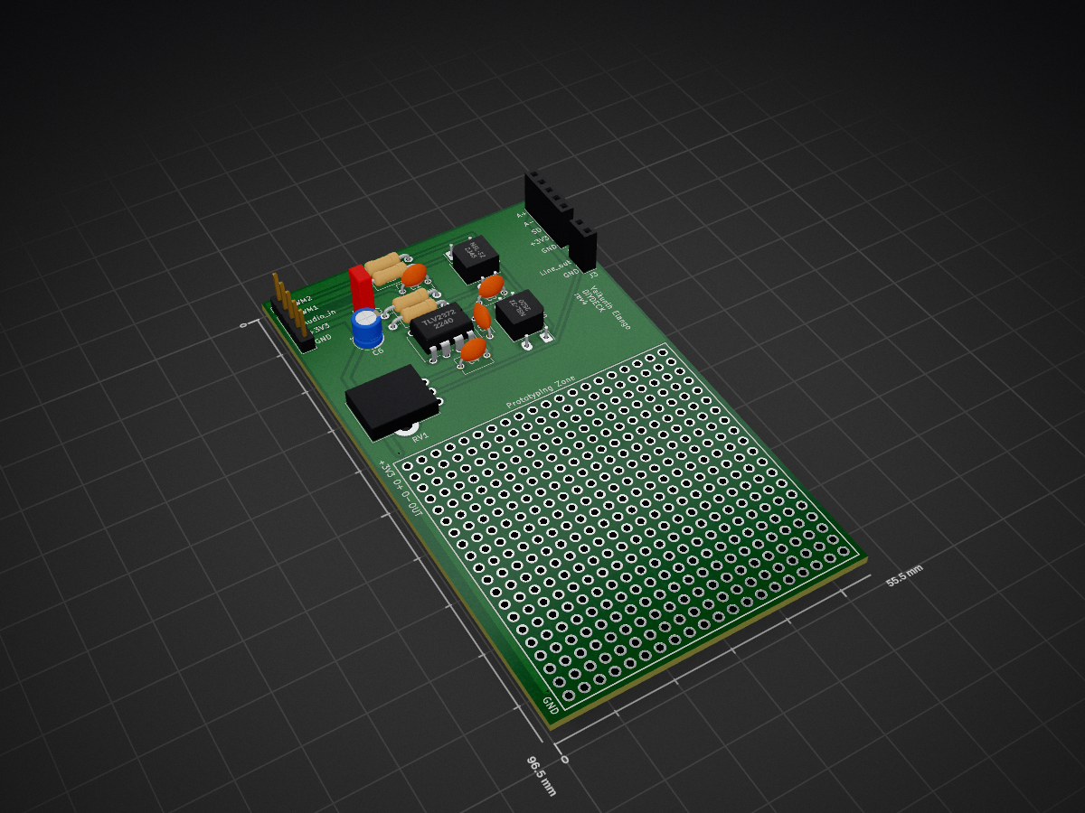
JDPDIYDECK is an open-source printed circuit board by vaikunth-e, from the vaikunth-e/DIYDECK repository on GitHub. It is a 2-layer board of 55.5 × 96.5 mm with 417 parts on 17 nets, routed with 80 tracks and 2 vias.
It is built around the TLV2372IP. Its parts include 6 capacitors, 4 resistors, 3 ICs and 3 connectors. It belongs with the audio and music boards of this library.
DIYDECK is a custom audio-processing board/system that takes an external audio signal, conditions it for an STM32 ADC, applies real-time embedded DSP effects, and outputs the processed signal through the STM32 DAC into the audio board/amplifier path.
Input audio is AC-coupled and biased around mid-supply so the STM32 ADC can sample the waveform safely. The firmware removes the measured DC bias, applies optional effects, recenters the signal around the DAC midpoint, and outputs it through DAC channel 1.
Signal chain:
Laptop / audio source
→ AC coupling and biasing
→ STM32 ADC input
→ real-time DSP
→ STM32 DAC output
→ PCB audio path / amplifier / speaker
src/main.cpp: ADC/DAC setup, audio ISR, effect toggles, timer setupsrc/encoder_control.cpp: rotary encoder decoding and PWM setting selectionlib/my_reverb: Freeverb-style reverb implementationlib/my_ringmod: ring modulation effectEach sample is read from the ADC, denoised slightly by masking noisy LSBs, centered by subtracting a moving DC estimate, optionally processed through reverb and/or ring modulation, clipped to the DAC range, and written to the DAC.
The rotary encoder selects one of 16 predefined cutoff settings. Each setting maps a target cutoff frequency to two PWM duty cycles used by the external board.
During bring-up, I debugged DC offset, clipping, low output volume, scratchiness, sample-rate instability, and ADC/DAC scaling. I used serial diagnostics and lab equipment including an oscilloscope, multimeter, function generator, and bench power supply to validate the signal path.
pio run
pio run --target upload
pio device monitor| Qty | Value | Footprint | References |
|---|---|---|---|
| 2 | 180 | Resistor_THT:R_Axial_DIN0207_L6.3mm_D2.5mm_P10.16mm_Horizontal | R3, R4 |
| 2 | 4.7nF | FA28X7R1H472KNU00:CAPRB500W50L400T250H550 | C2, C3 |
| 2 | 470k | Resistor_THT:R_Axial_DIN0207_L6.3mm_D2.5mm_P10.16mm_Horizontal | R1, R2 |
| 2 | 47uF | RDEC71E476MWK1H03B:CAP_RDEC71E476MWK1H03B | C1, C4 |
| 2 | NSL-32 | OptoDevice:Luna_NSL-32 | U1, U2 |
| 1 | 100nF | Capacitor_THT:C_Rect_L4.0mm_W2.5mm_P2.50mm | C7 |
| 1 | 100uF | Capacitor_THT:CP_Radial_D5.0mm_P2.00mm | C6 |
| 1 | 10k | Potentiometer_THT:Potentiometer_Bourns_PTV09A-1_Single_Vertical | RV1 |
| 1 | Conn_01x02 | Connector_PinSocket_2.54mm:PinSocket_1x02_P2.54mm_Vertical | J3 |
| 1 | Conn_01x05 | Connector_PinSocket_2.54mm:PinSocket_1x05_P2.54mm_Vertical | J2 |
| 1 | Conn_01x05 | Connector_PinHeader_2.54mm:PinHeader_1x05_P2.54mm_Vertical | J1 |
| 1 | TLV2372 | TLV2372IP:P8 | U3 |
The 17 most common of 417 parts.
It measures 55.5 × 96.5 mm and has 2 copper layers, 1.6 mm thick.
417 parts, built around the TLV2372IP. The full list of its parts is on this page, with links to each part's symbol and footprint where PCBKit's library has them.
From the vaikunth-e/DIYDECK repository on GitHub, at the commit this page was made from: the board is JDPDIYDECK_KICAD/JDPDIYDECK.kicad_pcb and its schematic JDPDIYDECK_KICAD/JDPDIYDECK.kicad_sch. PCBKit opens the board in the browser, with nothing to install.
Its repository states no licence, so its author keeps all rights: ask vaikunth-e before reusing the design.
Moragor/BatteryAnalyzer_MkII
Updated Version of the battery analyzer, now with constant current


devjamescollier/STM-32_Based_Waveform_Generator
USB-powered programmable function generator built around an STM32C031K6T6 microcontroller and MCP4901 DAC. Generates clean sine, triangle, and square waveforms with amplitude control via potentiometer, mode selection…

dnz1666/impedance-buffer-pcb
Analog circuit design (impedance buffer + LP filter) – KiCad schematic & PCB layout for a student EV project at RWTH Aachen


jensboe/Modellbahn
columns 1 block:selfmade block:base columns 1 nucleo adapter["adapter board A"] end space expansion1["expansion board A 1"] space expansionn["expansion board A n"] space expansionb["expansion board B"] adapter…

jkbkwcn/harm_meas_using_os
An electronic circuit project designed to measure mains current harmonics with amplitudes below one Least Significant Bit (LSB) of an Analog-to-Digital Converter.

JohnRipple/turbine-sensor
After taking a look at the kit it was lacking content. It could be built in about 10 minutes. With a 45 minute time slot for each class there was a lot of time to fill, so I decided to make a more interesting turbine…