
2 layers107 × 54 mm
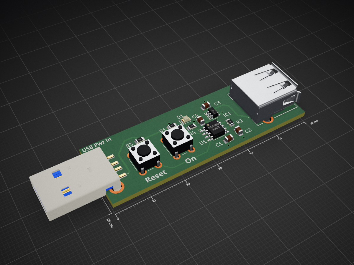
 tti0/USB-Monostable
An in-line timer/monostable switch for USB power
555-monostable usb switch rev2 is an open-source printed circuit board by tti0, from the tti0/USB-Monostable repository on GitHub, published under the CERN-OHL-P-2.0 licence. It is a 2-layer board of 60 × 20 mm with 15 parts on 14 nets, routed with 75 tracks and 8 vias.
It is built around the NE555D. Its parts include 4 capacitors, 4 resistors, 2 ICs, 2 connectors and 2 switches.
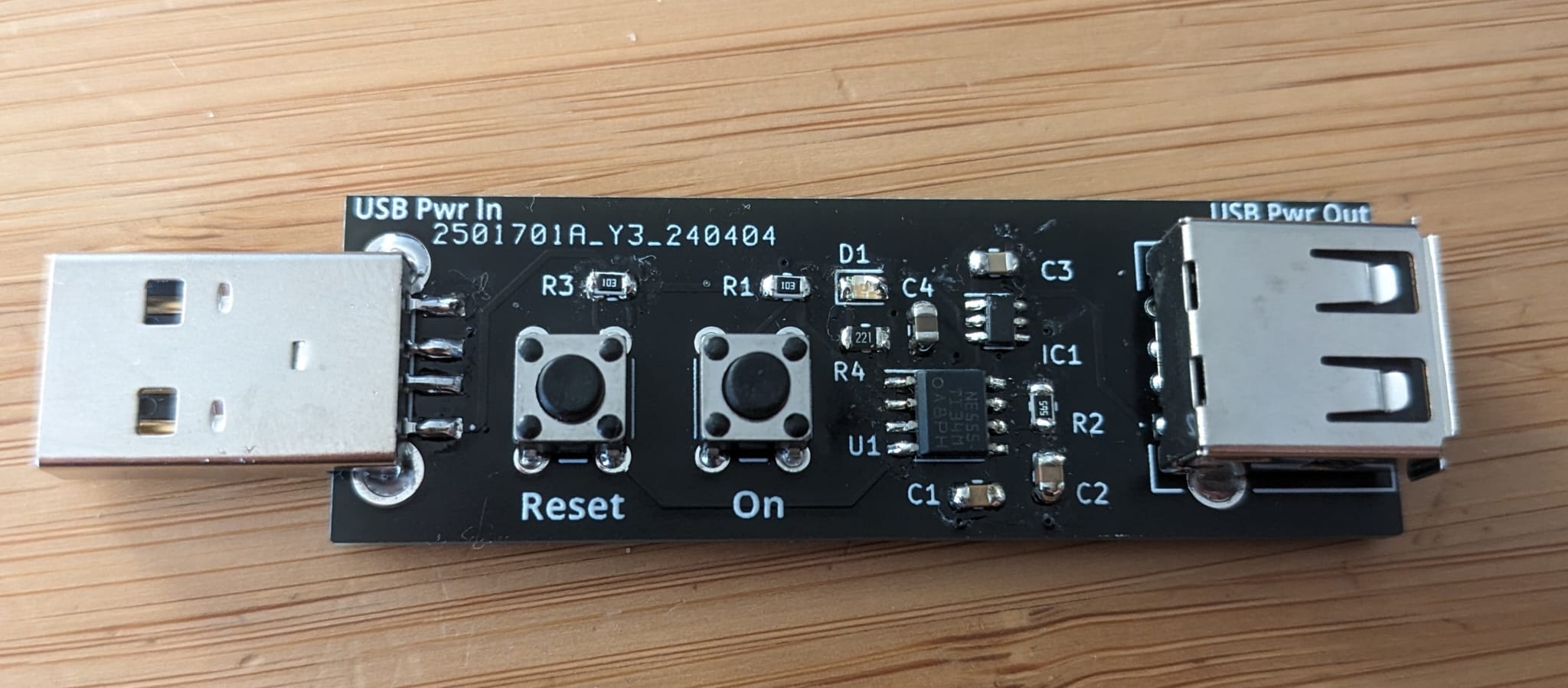
Populated USB-Monostable PCB
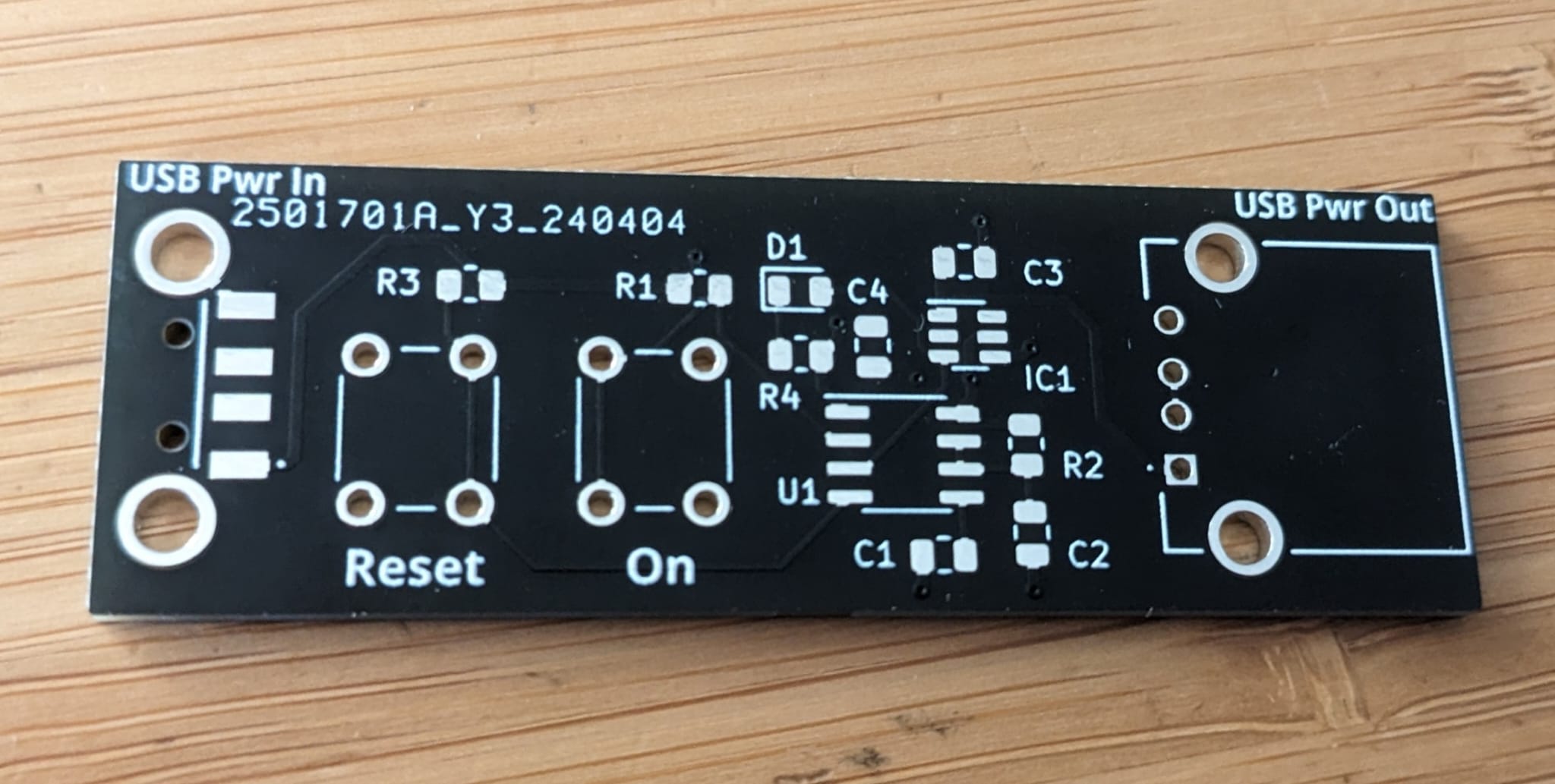
Unpopulated USB-Monostable PCB
PCBs can be purchased from any fabricator by submitting the latest Gerber files from this repository (see the Releases page). The footprints chosen (mostly SMD 0805) allow all components in the BOM to then be soldered by hand fairly easily. It is recommended to use lead-free solder of diameter 0.6 mm.
The values of R2 and C2 may be adjusted to alter the time period (the length of time for which power is supplied to the output after the button is pressed) of the switch. Since this project uses the 555 timer, the standard monostable equation applies:
Time period (seconds) = R2 (Ohms) * C2 (Farads) * 1.1The LED D1 and its current-limiting resistor R4 can be omitted during construction if a visual status indicator is not required.
The USB connectors J1 and J2 are the only non-standard footprints in this project. Proprietary KiCAD footprints can be downloaded by following the links in the below table, but cannot be distributed with this project for licensing reasons.
Values of R2 and C2 listed here result in a time period of 39.6 seconds.
| Reference | Qty | Value | Footprint |
|---|---|---|---|
| C1 | 1 | 10 nF | Capacitor_SMD:C_0805_2012Metric |
| C2 | 1 | 10 uF | Capacitor_SMD:C_0805_2012Metric |
| C3 | 1 | 100 nF | Capacitor_SMD:C_0805_2012Metric |
| C4 | 1 | 4.7 uF | Capacitor_SMD:C_0805_2012Metric |
| D1 | 1 | LED (Green) | LED_SMD:LED_0805_2012Metric |
| IC1 | 1 | SIP32508DT-T1-GE3 | Package_TO_SOT_SMD:SOT-23-6 |
| J1 | 1 | USB_A (Input, male) | SamacSys_Parts:USB1061GFLA |
| J2 | 1 | USB_A (Output, female) | SamacSys_Parts:USBASRA |
| R1, R3 | 2 | 10k | Resistor_SMD:R_0805_2012Metric |
| R2 | 1 | 3M6 | Resistor_SMD:R_0805_2012Metric |
| R4 | 1 | 1k | Resistor_SMD:R_0805_2012Metric |
| SW1 | 1 | SW_Push (Set) | Button_Switch_THT:SW_PUSH_6mm |
| SW2 | 1 | SW_Push (Reset) | Button_Switch_THT:SW_PUSH_6mm |
| U1 | 1 | NE555D | Package_SO:SOIC-8_3.9x4.9mm_P1.27mm |
This project is Copyright (c) tti0 2024, and licenced under the CERN Open Hardware Licence Version 2 – Permissive. Please see LICENSE for full details.
| Qty | Value | Footprint | References |
|---|---|---|---|
| 2 | 10k | Resistor_SMD:R_0805_2012Metric | R1, R3 |
| 1 | 10 nF | Capacitor_SMD:C_0805_2012Metric | C1 |
| 1 | 10 uF | Capacitor_SMD:C_0805_2012Metric | C2 |
| 1 | 100 nF | Capacitor_SMD:C_0805_2012Metric | C3 |
| 1 | 220 | Resistor_SMD:R_0805_2012Metric | R4 |
| 1 | 4.7 uF | Capacitor_SMD:C_0805_2012Metric | C4 |
| 1 | 5M6 | Resistor_SMD:R_0805_2012Metric | R2 |
| 1 | LED | LED_SMD:LED_0805_2012Metric | D1 |
| 1 | NE555D | Package_SO:SOIC-8_3.9x4.9mm_P1.27mm | U1 |
| 1 | SIP32508DT-T1-GE3 | Package_TO_SOT_SMD:SOT-23-6 | IC1 |
| 1 | SW_Push (Reset) | Button_Switch_THT:SW_PUSH_6mm | SW2 |
| 1 | SW_Push (Set) | Button_Switch_THT:SW_PUSH_6mm | SW1 |
| 1 | USB_A (Input, male) | SamacSys_Parts:USB1061GFLA | J1 |
| 1 | USB_A (Output, female) | SamacSys_Parts:USBASRA | J2 |
It measures 60 × 20 mm and has 2 copper layers, 1.6 mm thick.
15 parts, built around the NE555D. The full list of its parts is on this page, with links to each part's symbol and footprint where PCBKit's library has them.
From the tti0/USB-Monostable repository on GitHub, at the commit this page was made from: the board is 555-monostable-usb-switch-rev2.kicad_pcb and its schematic 555-monostable-usb-switch-rev2.kicad_sch. PCBKit opens the board in the browser, with nothing to install.
Its repository publishes it under the CERN-OHL-P-2.0 licence: you may reuse it on that licence's terms (keep the author's notice, and for a copyleft licence share your changes alike).

Millisman/EG8010
Collection of designs for the EG8010 (ASIC for single-phase SPWM control H-bridge)

Andre1Becker/GalvOS
Open-source ESP32-S3 laser show controller — built to replace proprietary OEM controllers in RGB galvo laser projectors


Robert-Mones/Claculator
A reverse Polish notation calculator with added features such as comparisons, branching, and custom recursive operators taken from the Clac project from the 15-122 course at Carnegie Mellon University.
