
2 layers45.7 × 31.8 mm
LEDx16 board
tardate/LittleArduinoProjects
a collection of "Little Electronic & Arduino Projects", most involving electronics or an Arduino in one way or another!
36 parts803MIT

 trickart/gameboy-camera-printer-shield
An Arduino Uno R4 WiFi shield (KiCad project) for dumping DMG/GBC cartridges — especially the Game Boy Camera — and printing to the Game Boy Pocket Printer.
Gameboy camera printer shield is an open-source printed circuit board by trickart, from the trickart/gameboy-camera-printer-shield repository on GitHub. It is a 2-layer board of 97.8 × 53.3 mm with 17 parts on 52 nets, routed with 215 tracks and 48 vias.
It is built around the 74HC595. Its parts include 6 connectors, 4 capacitors, 2 ICs and 1 resistor. It belongs with the retro computing and games boards of this library.
An Arduino Uno R4 WiFi shield (KiCad project) for dumping DMG/GBC cartridges — especially the Game Boy Camera — and printing to the Game Boy Pocket Printer.
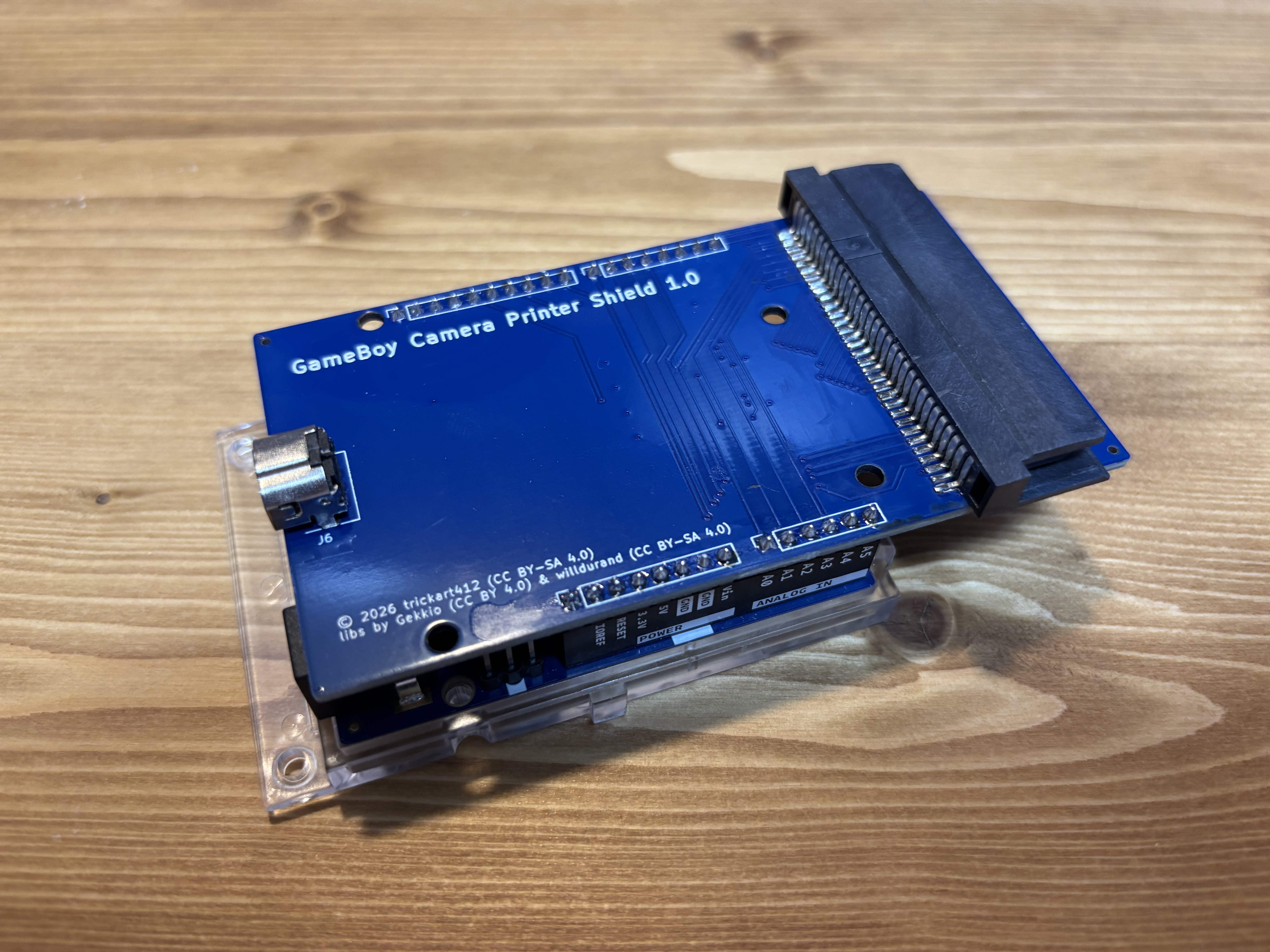
With an Arduino Uno R4 WiFi (5V logic, RA4M1) this shield lets you:
.sav fileKey design points:
| Path | Description |
|---|---|
gameboy-camera-printer-shield.kicad_pro/.kicad_sch/.kicad_pcb | KiCad project, schematic, and PCB layout |
Arduino_MountingHole.pretty/ | Custom footprint library |
jlcpcb/gerber/ | Gerber and drill files |
jlcpcb/production_files/ | BOM, CPL, and zipped Gerbers for JLCPCB assembly |
Opening the schematic/PCB requires these external KiCad libraries in addition to the bundled Arduino_MountingHole.pretty:
Clone them and register the symbol/footprint libraries in KiCad (Preferences → Manage Symbol/Footprint Libraries) before opening the project.
| Part | Designator | Spec | Qty |
|---|---|---|---|
| 74HC595 | U1, U2 | Shift registers for address lines A0–A15 (TSSOP-16) | 2 |
| DMG cartridge connector | J5 | 32-pin, 2 mm pitch | 1 |
| GB link port | J6 | MGB link connector for the printer | 1 |
| Ceramic capacitor 0.1 µF | C1, C2, C3 | Decoupling (each 74HC595 + cartridge VCC) | 3 |
| Capacitor 10 µF | C4 | Bulk capacitance on the cartridge VCC rail | 1 |
| Resistor 10 kΩ | R1 | Pull-up on cartridge /RST | 1 |
| Pin sockets | J1–J4 | Arduino Uno shield headers (8/10/6/8 pins) | 4 |
No level shifters or crystal oscillator needed — PHI is just toggled statically Low/High from a GPIO; no clock generation is required.
| Arduino pin | Function |
|---|---|
| D0–D7 | Data bus D0–D7 (bidirectional) |
| D10 | 74HC595 ST_CP (latch) |
| D11 (COPI/MOSI) | 74HC595 DS (serial data in) |
| D13 (SCK) | 74HC595 SH_CP (shift clock) |
| A0 | Cartridge PHI (pin 2) — ★ required for the Camera |
| A1 | Cartridge /WR (pin 3) |
| A2 | Cartridge /RD (pin 4) |
| A3 | Cartridge /CS (pin 5) |
| D8 | Printer SCK (link pin 5) |
| D9 | Printer SOUT (link pin 3 = printer SIN) |
| D12 | Printer SIN (link pin 2 = printer SOUT) |
| A4 / A5 | Unused |
| 595 pin | Signal | Connects to |
|---|---|---|
| 16 | VCC | 5V |
| 8 | GND | GND |
| 13 | /OE | GND (output always enabled) |
| 10 | /MR | 5V (reset always released) |
| 11 | SH_CP | Arduino D13 |
| 12 | ST_CP | Arduino D10 |
| 14 (U1) | DS | Arduino D11 |
| 9 (U1) | Q7′ | Cascades to pin 14 (DS) of U2 |
595 outputs: Q0 = pin 15, Q1–Q7 = pins 1–7.
| 595 | Output pins | Signal | Cartridge pins |
|---|---|---|---|
| U1 | 15, 1, 2, 3, 4, 5, 6, 7 | A0–A7 | 6–13 |
| U2 | 15, 1, 2, 3, 4, 5, 6, 7 | A8–A15 | 14–21 |
(Bit order: Q0 = LSB. Sending the high byte first, then the low byte over SPI puts the low byte in U1 and the high byte in U2.)
| Arduino | Dir | Cartridge pin | Signal |
|---|---|---|---|
| D0–D7 | ⇄ | 22–29 | D0–D7 (bidirectional data) |
| A0 | → | 2 | PHI (Camera ROM/RAM enable) |
| A1 | → | 3 | /WR |
| A2 | → | 4 | /RD |
| A3 | → | 5 | /CS |
| 5V | → | 1 | VCC |
| GND | → | 32 | GND |
| 10 kΩ → 5V | → | 30 | /RST (fixed pull-up) |
| — | NC | 31 | AUDIO (unconnected) |
Rule of thumb: 0.1 µF right at each IC's power pins, plus one 10 µF on the power rail.
| Capacitor | Value | Placement |
|---|---|---|
| Decoupling | 0.1 µF | 74HC595 U1: shortest path across pin 16 (VCC) ↔ pin 8 (GND) |
| Decoupling | 0.1 µF | 74HC595 U2: shortest path across pin 16 (VCC) ↔ pin 8 (GND) |
| Decoupling | 0.1 µF | Cartridge: pin 1 (VCC) ↔ pin 32 (GND), right at the connector |
| Bulk | 10 µF | 5V–GND rail near the cartridge (smooths current spikes during reads) |
Keep the 0.1 µF caps as close as possible to the IC/connector pins — long leads defeat the purpose. The circuit will work without them, but they provide noise margin and dump stability.
| Link pin | Signal | Arduino |
|---|---|---|
| Pin 2 | SOUT (printer → Arduino) | D12 |
| Pin 3 | SIN (Arduino → printer) | D9 |
| Pin 5 | SCK (Arduino is master) | D8 |
| Pin 6 | GND | GND |
The Arduino acts as clock master and bit-bangs SPI mode 3 (SCK idles High, data updated on the falling edge, sampled on the rising edge, MSB first) at ~8 kHz.
| Operation | /RD | /WR | /CS | PHI |
|---|---|---|---|---|
| ROM read (header/logo/ROM) | Low | High | Low | Low |
| SRAM read (photos, 0xA000–0xBFFF) | Low | High | Low | High |
| Register write (RAM enable / bank select) | High | Low (pulse) | High | Low |
0x0A to 0x0000 (enable RAM)0x00–0x0F to 0x4000 (select RAM bank)0xA000–0xBFFF0x00 to 0x0000 (disable RAM)Concatenate the hex dump on a PC and convert it with bytes.fromhex() into a 131,072-byte .sav file. Photos can then be extracted with a GB Camera save viewer or an emulator.
Ready-to-order files for JLCPCB are in jlcpcb/production_files/ (Gerber zip, BOM, and CPL for SMT assembly).
This project is licensed under CC BY-SA 4.0.
The parts derived from the external libraries listed in Required Libraries (Gekkio/gekkio-kicad-libs and willdurand/kicad-libs) remain subject to their respective licenses.
| Qty | Value | Footprint | References |
|---|---|---|---|
| 4 | MountingHole_3.2mm | Arduino_MountingHole:MountingHole_3.2mm | MH1, MH2, MH3, MH4 |
| 3 | 0.1u | Capacitor_SMD:C_0603_1608Metric | C1, C2, C3 |
| 2 | 74HC595 | Package_SO:TSSOP-16_4.4x5mm_P0.65mm | U1, U2 |
| 1 | 10k | Resistor_SMD:R_0603_1608Metric | R1 |
| 1 | 10u | Capacitor_SMD:C_0805_2012Metric | C4 |
| 1 | Analog | Connector_PinSocket_2.54mm:PinSocket_1x06_P2.54mm_Vertical | J3 |
| 1 | Digital/PWM | Connector_PinSocket_2.54mm:PinSocket_1x08_P2.54mm_Vertical | J4 |
| 1 | Digital/PWM | Connector_PinSocket_2.54mm:PinSocket_1x10_P2.54mm_Vertical | J2 |
| 1 | GB_GBC_1x32 | willdurand_connector:GB_GBC_1x32 | J5 |
| 1 | GameBoy_LinkPort | Gekkio_Connector:GameBoy_LinkPort_MGB_Horizontal | J6 |
| 1 | Power | Connector_PinSocket_2.54mm:PinSocket_1x08_P2.54mm_Vertical | J1 |
It measures 97.8 × 53.3 mm and has 2 copper layers, 1.6 mm thick.
17 parts, built around the 74HC595. The full list of its parts is on this page, with links to each part's symbol and footprint where PCBKit's library has them.
From the trickart/gameboy-camera-printer-shield repository on GitHub, at the commit this page was made from: the board is gameboy-camera-printer-shield.kicad_pcb and its schematic gameboy-camera-printer-shield.kicad_sch. PCBKit opens the board in the browser, with nothing to install.
Its repository states no licence, so its author keeps all rights: ask trickart before reusing the design.
tardate/LittleArduinoProjects
a collection of "Little Electronic & Arduino Projects", most involving electronics or an Arduino in one way or another!

ChrisChrisLoLo/beyblock20
The magnetic, modular, 20-key macropad that can join together to form an ortholinear board

slu4coder/Minimal-64x4-Home-Computer
My DIY TTL home computer with VGA and PS/2 and 4x the processing power of a Commodore C64 or Apple II.

electroniceel/protoboard
Advanced protoboard layout with 1.27mm pitch for smd parts

TobleMiner/DC-UPS
A small DC UPS, designed to keep small appliances like consumer network equipment running during power outages


