


4 layers234 × 84 mm
Main panel
google/mozc-devices
Circuit diagrams and firmware source code for Gboard DIY keyboards
234 parts3kApache-2.0

 tomsaleeba/ergoslab18
Design files for a 52-key, split, columnar staggered mechanical keyboard
Ergoslab is an open-source printed circuit board by tomsaleeba, from the tomsaleeba/ergoslab repository on GitHub, published under the MIT licence. It is a 2-layer board of 114.5 × 101.2 mm with 102 parts on 55 nets, routed with 1,018 tracks and 89 vias.
It is built around the SK6812MINI-E. Its parts include 26 diodes, 26 switches, 5 connectors and 2 resistors. It belongs with the keyboards and input boards and the AVR (ATmega, ATtiny) boards of this library.
a columnar stagged keyboard that uses a combination of Cherry MX (or compatible) and Kailh choc switches to pack in a heap of thumb keys
Update Dec 2020: I've been using this keyboard full time (I'm a professional software developer so it sees a lot of use) for a year now and I'm still in love with it. If you're considering making one, I would call this design battle proven now.
Update Jan 2022: Still using this full-time and loving it 💪.
Before swapping to this keyboard, I had been using an ErgoDox Infinity and an EZ as my daily drivers for quite a few years. I loved using them but I was looking for something more compact and with more (easily accessible) thumb keys. There are so many candidates (here, here, here and here) but none match exactly what I want, so I decided build my own!
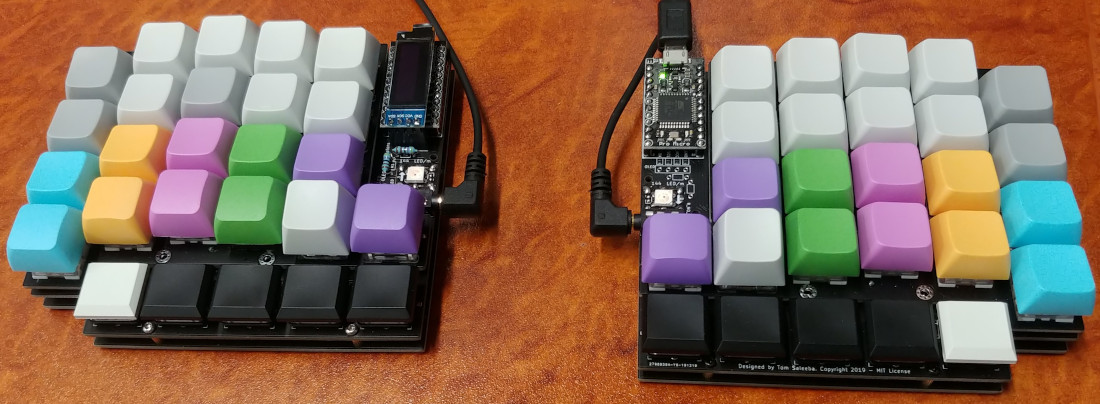
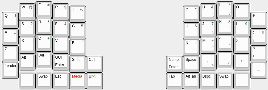
See the guide here.
See the releases for this GitHub repo for the generated Gerber files. You probably want the most recent version.
If you need to generate your own gerbers, see how to turn the master PCB into the 3 generated PCBs and then how to generate gerbers.
Note1: the screw/bolt length depends on the height of the standoffs you get. You want 1.6mm thick PCBs so make sure you don't have too much thread on your screws.
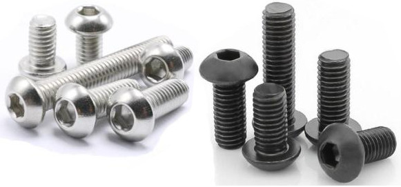
Note2: it's highly recommended to get hex head/allen key/ISO7380 screws (see image below). This is because a phillips head screwdriver probably won't fit through the holes in the switch plate to tighten the screws on the middle/PCB layer. You can always drill those holes a bit bigger or loctite the screws in (so they won't need tighening) to workaround this. As you have hotswap sockets, you may be able to remove the switches and pull the middle/PCB layer screws out through the switch holes. Beware: with 4mm long screws, I couldn't achieve this, though it was very close.
These are the parts you can order from LCSC at the same time as having your PCBs manufactured. The listed quantity is to assemble both halves.
| QTY | Description | LCSC Part No |
|---|---|---|
| 0/2/4 | 4.7KO (4701) ±1% (2 per OLED) | C58678 |
| 2 | PJ-3200B-4A TRRS Connector | C136687 |
| 2 | Switch 5.25.21.5 reset switch | C92584 |
| 2 | 2.54mm 1*40P round Female header | C9811 |
| 0/1/2 | OLED Female header | C124413 |
| 52 | 1N4148 Switching Diode | C14516 |
| 18 | M2x6mm standoffs (See Note3) for middle/PCB layer to base plate mounting | M2x6 |
Note3: the standoffs between the middle/PCB layer and the base plate can be quite small, probably as small as 3mm. The problem with that is making sure the bolts engage the threads enough. Feel free to experiment with getting a super slim keyboard. Perhaps use a long bolt, a threadless spacer and a nut?
Contributions are welcome. I'm not selling these keyboards and I already have two for myself so I can't afford to manfacture more PCBs to test changes. If you make changes to the PCB design, ideally you would confirm it all works by manufacturing your own PCBs.
Steps for contributing:
We edit a single PCB file that contains the information required to generate all 3 layers (switch plate, circuitry, base) of a sandwich case keyboard. Keeping it all in one file ensures that things like mounting holes always stay lined up.
There is some magic in the settings of items on the PCB to indicate what layer they belong on. Read the code for the specifics but as a general guide:
You must have Kicad installed in your system. Doing this makes the pcbnew
python module available. Make sure you don't have any virtualenv, etc activated
as you need to be using you system-wide python. Check for the module by running
the following in the python REPL:
import pcbnewNow you can regenerate the PCBs with:
python ./generate_pcbs.pyNormally keeping generated things in source control is not a good idea but in the interest of keeping things easy, we include the generated PCBs.
Using KiCad 5.1.4, here's the settings to generate gerbers.
Plot settings (should be the defaults):
Plot format: Gerber
Included layers:
  F.Cu
  B.Cu
  F.Paste
  B.Paste
  F.SilkS
  B.SilkS
  F.Mask
  B.Mask
  Edge.Cuts
Plot foorprint values: yes
Plot footprint references: yes
Exclude PCB edge layer from other layers: yes
Exclude pads from silkscreen: yes
Default line width: 0.1mm
Coordinate format: 4.6, unit mm
Drill settings:
Drill File Format: Excellon
Mirror Y axis: no
Minimal header: no
PTH and NPTH in single file: no
Oval Holes Drill Mode: Use alternate drill mode
Map File Format: PostScript
Drill Origin: Absolute
Drill Units: Inches
Zeros Format: Suppress leading zeros
The fix for the JLCPCB PTH layer error was to change the oval hole drill mode.
How portable is it? It weighs 360grams (180grams for each half) with cheap DSA plastic keycaps. It measures 115mm x 102mm and with 6mm standoffs, it's 16mm to the top of the switch plate or 31mm to the top of DSA keycaps, including the height of rubber bump-ons. I'll let you decide how portable you think that is but it was designed to be portable.
Is I2C between the halves supported? Sort of. The OLED screens use I2C so you won't be able to use them. Also there's no solder jumpers so you'll have to jump some wires between the OLED header SDA/SCL pins and the SLAVE_LED pin/data pin on the unused TRRS jack. This isn't an intended use but you can certainly hack it, check the schematic for details.
What happened to a single PCB that works as all 3 layers? Originally I tried to make one PCB design that works as all 3 layers of a sandwich design: base, PCB and switch plate. The idea was taken from for-split-keyboard and mitosis. I failed because I wanted to have minimal post-manufacture cutting by hand and JLCPCB kept rejecting my desgins as they didn't have strong enough supports to hold the PCB together though the whole manufacture process. So now we have "master" PCB design and use a python script to generate the PCBs for each layer from that master.
Do you have keyboard-layout-editor source?
Yes. Either this file in this repo or here's a (hopefully up to date)
permalink
Do you have a vector of the right hand "plate"?
Yep, see misc/ergoslab-right.svg.
| Qty | Value | Footprint | References |
|---|---|---|---|
| 26 | 1N4148 | Diode_THT:D_DO-35_SOD27_P7.62mm_Horizontal | D0:0, D0:1, D0:2, D0:3, D0:4, D1:0, D1:1, D1:2, D1:3, D1:4, D2:0, D2:1, D2:2, D2:3, D2:4, D3:0 +10 |
| 21 | SW_Push | footprints:Kailh_socket_reversible | SW0:0, SW0:1, SW0:2, SW0:3, SW0:4, SW1:0, SW1:1, SW1:2, SW1:3, SW1:4, SW2:0, SW2:1, SW2:2, SW2:3, SW2:4, SW3:0 +5 |
| 11 | MountingHole_2.2mm_M2_Pad_Via | MountingHole:MountingHole_2.2mm_M2_Pad_Via | Mount0, Mount1, Mount2, Mount3, Mount4, Mount5, Mount6, Mount7, MountNotTop0, MountNotTop3, MountNotTop4 |
| 10 | switchplate-brace | footprints:switchplate-brace | Brace0, Brace1, Brace2, Brace3, Brace4, Brace5, Brace6, Brace7, BraceNotTop0, BraceNotTop1 |
| 5 | SW_Push | footprints:kailh-choc-solder-reversible | SW4:1, SW4:2, SW4:3, SW4:4, SW4:5 |
| 2 | 4k7 | footprints:resistor | R1, R2 |
| 2 | SK6812mini | footprints:ws2812-single | LED_L1, LED_R1 |
| 2 | SW_Push | footprints:SW_TACT_ALPS_SKQGABE010 | SW-reset2, SW-reset3 |
| 2 | VAL** | footprints:HOLE_M2 | MountNotTop1, MountNotTop2 |
| 1 | ICSP | footprints:PinHeader_1x06_P2.54mm_Vertical | P2 |
| 1 | LOGO | footprints:chicken | CHICKEN |
| 1 | L_B_LED | footprints:ws2812-strip | J1 |
| 1 | L_GND | footprints:Jumper | JP1 |
| 1 | L_NO_B_LED | footprints:Jumper | JP10 |
| 1 | L_NO_F_LED | footprints:Jumper | JP9 |
| 1 | L_SCL | footprints:Jumper | JP3 |
| 1 | L_SDA | footprints:Jumper | JP4 |
| 1 | L_VCC | footprints:Jumper | JP2 |
| 1 | MJ-4PP-9 | footprints:TRRS-helix | TRRS1 |
| 1 | OLED | footprints:oled_header_helix | P1 |
| 1 | ProMicro | footprints:Pro_Micro_ergotravel | PM1 |
| 1 | R_B_LED | footprints:ws2812-strip | J2 |
| 1 | R_GND | footprints:Jumper | JP8 |
| 1 | R_NO_B_LED | footprints:Jumper | JP11 |
| 1 | R_NO_F_LED | footprints:Jumper | JP12 |
| 1 | R_SCL | footprints:Jumper | JP6 |
| 1 | R_SDA | footprints:Jumper | JP5 |
| 1 | R_VCC | footprints:Jumper | JP7 |
| 1 | SLAVE_LED | footprints:PinHeader_1x01_P2.54mm_Vertical | J3 |
| 1 | SW_Push | footprints:TACT_SWITCH_TVBP06 | SW-reset1 |
It measures 114.5 × 101.2 mm and has 2 copper layers, 1.6 mm thick.
102 parts, built around the SK6812MINI-E. The full list of its parts is on this page, with links to each part's symbol and footprint where PCBKit's library has them.
From the tomsaleeba/ergoslab repository on GitHub, at the commit this page was made from: the board is pcb/ergoslab.kicad_pcb. PCBKit opens the board in the browser, with nothing to install.
Its repository publishes it under the MIT licence: you may reuse it on that licence's terms (keep the author's notice, and for a copyleft licence share your changes alike).
google/mozc-devices
Circuit diagrams and firmware source code for Gboard DIY keyboards

Bastardkb/Dilemma
The Dilemma is a vertical stagger low-profile keyboard with mods.

Pwnsat/FlatSat
Flatsat v1.0 is a hardware based platform for aerospace cybersecurity research

adamws/kicad-kbplacer
KiCad plugin for automatic keyboard's key placement and routing

imchipwood/dumbpad
Simple 4x4 numpad with rotary encoder. Powered by QMK via ATmega32u4 Pro Micro

makerforgetech/modular-biped
An open source framework for creating a bipedal modular companion robot.

