4 layers37 × 34.3 mm
Readout 60pin
opentac/opentac
OpenTac: open tools to design, fabricate, read and simulate flex-PCB tactile skins that sense normal and shear force, for any robot surface.
55 parts92MIT
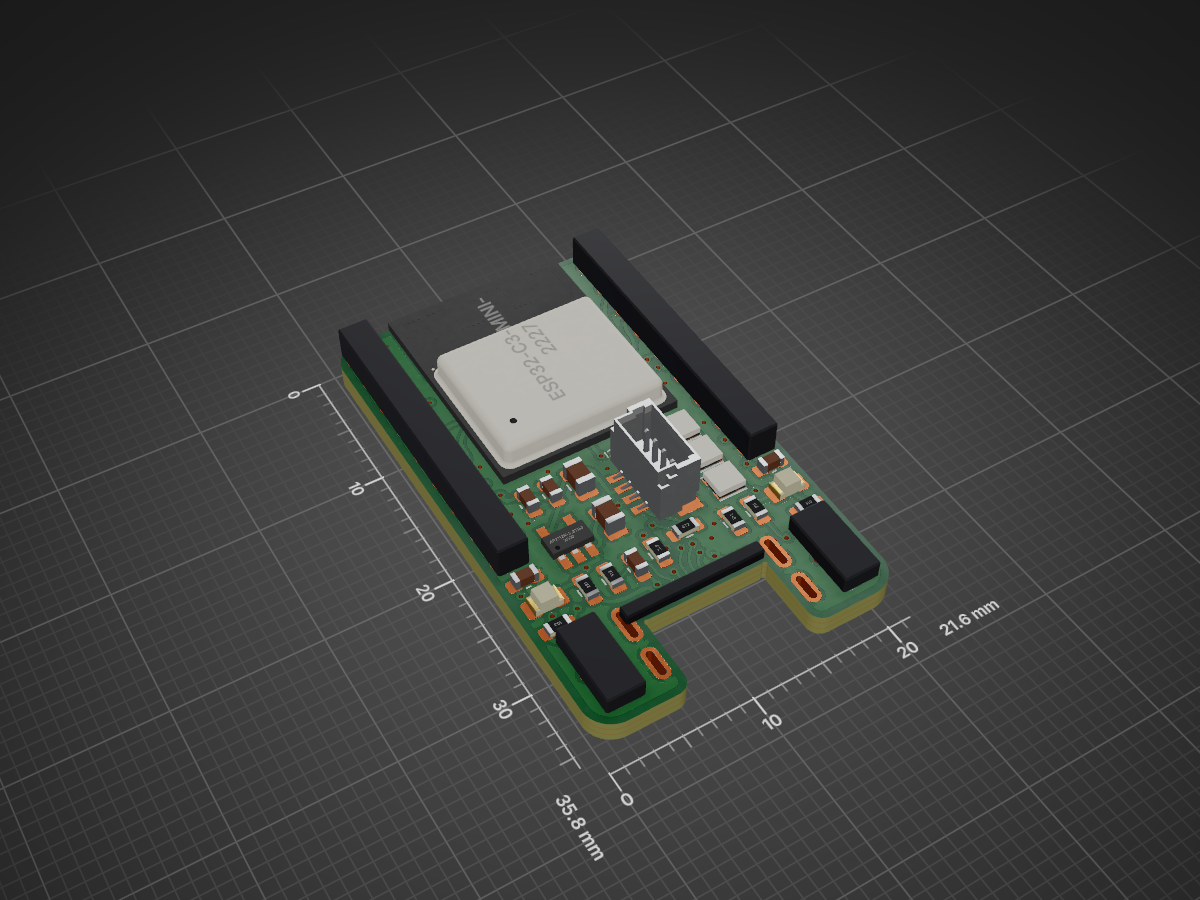
 toby-alpha/transparent-devboard1
The Dev Board is based off the ESP32 C3 Mini module. It contains a USB-C port, power LED, user LED, 3x WS2812B 2020 Adressable LEDs, >6V voltage input, as well as all GPIO being broken out.
DevBoard ESP32-rounded is an open-source printed circuit board by toby-alpha, from the toby-alpha/transparent-devboard repository on GitHub. It is a 4-layer board of 21.6 × 35.8 mm with 30 parts on 44 nets, routed with 888 tracks and 67 vias.
It is built around the AP2112K-3.3TRG1, XL-2020RGBC-WS2812B and TSA343G00D-250J2, with the BM04B-SRSS-TB(LF)(SN) and GT-USB-7058 among its other parts. Its parts include 8 resistors, 7 capacitors, 5 diodes, 3 connectors and 2 ICs. It belongs with the microcontroller boards boards and the ESP32 and RISC-V boards of this library.


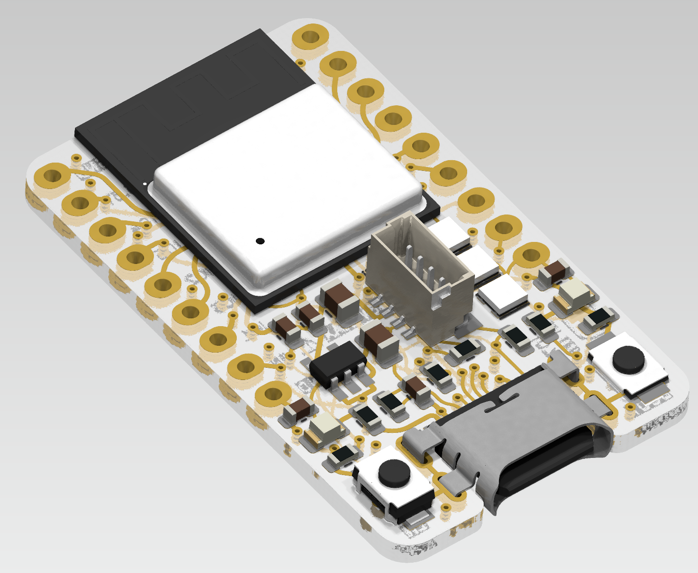
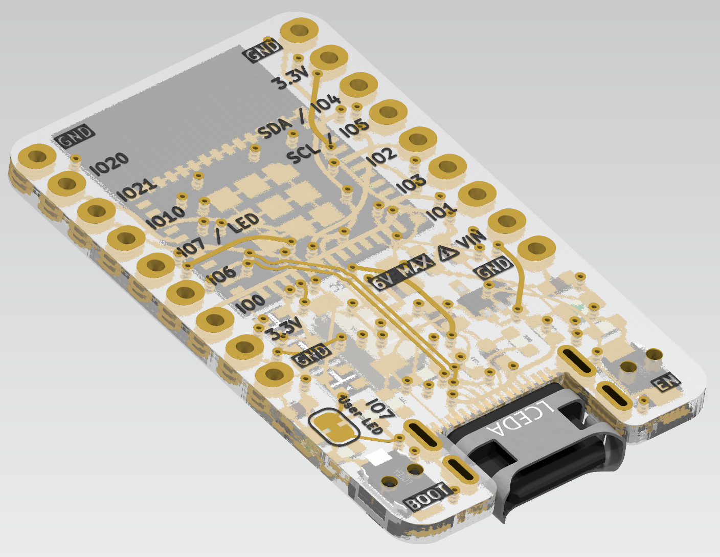
The Dev Board is based off the ESP32 C3 Mini module. It contains a USB-C port, power LED, user LED, 3x WS2812B 2020 Adressable LEDs, >6V voltage input, as well as all GPIO being broken out. The USB-C connector is inline to conform to a slim profile. It also has a JST SH connector for i2C connections.
It's specially manufactured from a transparent FR4 material to give it's unique look.
I was really intrigued with the concept of a transparent PCB, after seeing a JLCPCB advertisement for it. This prompted me to create an ESP devboard, that would be useful in many scenarios, while also exploring this new technology. The PCB also serves as a great method of education, showing inside of the complex electronics.
| Item | Cost (AUD) | Cost (USD) | Source | Link |
|---|---|---|---|---|
| Components Parts | 45 | 29 | LCSC | PDF Quote Upon Request |
| Hot Plate | 34 | 22 | Aliexpress | https://www.aliexpress.com/item/1005008125355441.html |
| Misc (Solder Paste.. Etc) | 30 | 19.5 | Aliexpress | |
| PCB + Stencil | 15 | 9.75 | JLCPCB | |
| Total | 81 |
| Qty | Value | Footprint | References |
|---|---|---|---|
| 4 | 100nF | Capacitor_SMD:C_0603_1608Metric | C2, C5, C6, C8 |
| 3 | XL-2020RGBC-WS2812B | EASYEDA2KICAD:LED-SMD_4P-L2.0-W2.0-BR-1 | LED1, LED2, LED3 |
| 2 | 10k | Resistor_SMD:R_0603_1608Metric | R6, R7 |
| 2 | 10uF | Capacitor_SMD:C_0805_2012Metric | C1, C3 |
| 2 | 4.7k | Resistor_SMD:R_0603_1608Metric | R2, R8 |
| 2 | 5.1k | Resistor_SMD:R_0603_1608Metric | R1, R3 |
| 2 | Conn_01x09_Pin | Connector_PinSocket_2.54mm:PinSocket_1x09_P2.54mm_Vertical | J1, J2 |
| 2 | TSA343G00D-250J2 | EASYEDA2KICAD:SW-SMD_L4.0-W2.9-P4.15-EH | SW1, SW2 |
| 1 | 100 | Resistor_SMD:R_0603_1608Metric | R4 |
| 1 | 1uF | Capacitor_SMD:C_0603_1608Metric | C4 |
| 1 | 220 | Resistor_SMD:R_0603_1608Metric | R5 |
| 1 | AP2112K-3.3TRG1 | EASYEDA2KICAD:SOT-25-5_L2.9-W1.6-P0.95-LS2.8-BL | U2 |
| 1 | BM04B-SRSS-TB(LF)(SN) | EASYEDA2KICAD:CONN-SMD_BM04B-SRSS-TB | CN1 |
| 1 | Blue LED | LED_SMD:LED_0805_2012Metric | D1 |
| 1 | ESP32-C3-MINI-1-H4(4MB) | EASYEDA2KICAD:WIFIM-SMD_ESP32-C3-MINI-1 | U1 |
| 1 | GT-USB-7058 | EASYEDA2KICAD:USB-C-SMD_GT-USB-7058 | USB1 |
| 1 | Green LED | LED_SMD:LED_0805_2012Metric | D2 |
| 1 | LOGO | LOGO | G*** |
| 1 | SolderJumper_2_Bridged | Jumper:SolderJumper-2_P1.3mm_Bridged_RoundedPad1.0x1.5mm | JP1 |
It measures 21.6 × 35.8 mm and has 4 copper layers, 1.6 mm thick.
30 parts, built around the AP2112K-3.3TRG1, XL-2020RGBC-WS2812B, TSA343G00D-250J2 and BM04B-SRSS-TB(LF)(SN). The full list of its parts is on this page, with links to each part's symbol and footprint where PCBKit's library has them.
From the toby-alpha/transparent-devboard repository on GitHub, at the commit this page was made from: the board is KiCAD Files/DevBoard ESP32-rounded.kicad_pcb and its schematic KiCAD Files/DevBoard ESP32-rounded.kicad_sch. PCBKit opens the board in the browser, with nothing to install.
Its repository states no licence, so its author keeps all rights: ask toby-alpha before reusing the design.
opentac/opentac
OpenTac: open tools to design, fabricate, read and simulate flex-PCB tactile skins that sense normal and shear force, for any robot surface.


benwys/SparrowHawk
Open source flight controller for FPV drones. Includes two complete hardware designs (kicad) with production files. Will include custom firmware (bare-metal cpp). In progress :-)

Eniemooo/Sensor-HAT
Open-hardware indoor air sensor (CO2, VOC/NOx, T/RH, light, sound): HAT for Raspberry Pi or standalone with Seeed XIAO + ESPHome. KiCad 10.

joshuata/impresence-esphome
An open-source, ESPHome-based room presence sensor built around the Hi-Link HLK-LD2460 mmWave radar and a Seeed Studio XIAO ESP32-S3.

Tinkerbug-Robotics/TinkerRocket
Model rocket flight computer, ground station, iOS app, and simulation

