2 layers156.2 × 97.8 mm

 TheJustMoose/74HCPU2
Handmade CPU. See README.md
CMD DEC is an open-source printed circuit board by TheJustMoose, from the TheJustMoose/74HCPU repository on GitHub. It is a 2-layer board of 78.7 × 50.8 mm with 37 parts on 51 nets, routed with 464 tracks and 1 via.
It is built around the 74HC00D, 74LS139PC and 74LS85DC. Its parts include 19 connectors, 6 ICs, 5 capacitors, 3 resistors and 1 diode.


Not a very scary instruction set discrete logic processor.
ASM UEMUL [blocked]
The words 'instruction' and 'command' mean the same thing.
|----------------------------------------------|f|-------------------------------------------------------------|
|   HIGH BYTE    |    LOW BYTE   |  HIGH BYTE  |l|                                                             |
|F E D C  B A 9 8 7 6 5 4 3 2 1 0|   (again)   |a|                    SHORT DESCRIPTION                        |
|   4   +   3 + 1 + 3  +    5    = 16          |g|                                                             |
|----------------------------------------------|s|-------------------------------------------------------------|
|   ADD |  DST |1|    CONST or   | 01 0000 0001|*| Add a constant to a register (This is one command, not two) |
|   ADD |  DST |0| SRC |-|Z|z|I|i| 00 0000 0000|*| Add a register to a register (same OpCode, different bit 8) |
|----------------------------------------------| |-------------------------------------------------------------|
|  ADDC |  DST |C| SRC |F|Z|z|I|i| 10 0001 0000|*| ADD a constant or register and CARRY FLAG to a register     |
|   AND |  DST |C| SRC |-|Z|z|I|i| 20 0010 0000|*| Bitwise AND a constant or register with a register          |
|    OR |  DST |C| SRC |-|Z|z|I|i| 30 0011 0000|*| Bitwise OR a constant or register with a register           |
|   XOR |  DST |C| SRC |-|Z|z|I|i| 40 0100 0000|*| Bitwise XOR a constant or register with a register          |
|   MUL |  DST |C| SRC |-|Z|z|I|i| 50 0101 0000|*| MULtiply a constant or register by a register.              |
|   UNO |  DST |0|-|TYP|F|-|-|-|-| 60 0110 0000|*| Unary commands INV, SWAP, LSR, LSRC                         |
|   MOV |  DST |C| SRC |*|Z|z|I|i| 70 0111 0000| | MOV a constant or register to a register                    |
|   LPM |  DST |0|EXT|D|U|-|-|-|W| 80 1000 0000| | Load Program Memory - Read data from [commands] ROM         |
|    LD |  DST |V|EXT|D|U|OFFSET4| 90 1001 0000| | LoaD data from RAM to a register                            |
|    IN |  DST |  PORT   |Z|z|I|i| A0 1010 0000| | INput data from port to a register                          |
|--------------|8-7-6-5-4|-------|-------------| |-------------------------------------------------------------|
|   OUT | PORT |1|    CONST or   | B1 1011 0001| | Output const to a port (This is one command, not two)       |
|   OUT | PORT |0| SRC |PRT|X|O|o| B0 1011 0000| | Output register to a port (same OpCode, different bit 8)    |
|----------------------------------------------| |-------------------------------------------------------------|
|    ST |  SRC |V|EXT|D|U|OFFSET4| C0 1100 0000| | STore a register to a RAM                                   |
| CMP | DST |C| SRC |-| - | D0 1101 0000|+| CoMPare a constant or register with a register |* - means ZF, CF, HCF flags, + - means GF, EQ, LF flags
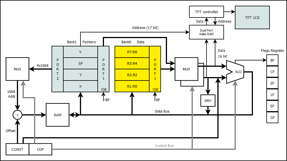
74HCPU has two register banks. First bank has 8 arithmetic registers. Second bank has 4 pointers (which can be used as 8 arithmetic registers). You can change the active bank by writing BF bit of the flags register.
| Name | Name |
|---|---|
| R7 | R6 |
| R5 | R4 |
| R3 | R2 |
| R1 | R0 |
|
|
Also, you can use the registers of bank 1 in the same way as bank 0: R0, R1, ... R7 (R7 will store the high half of SP, R6 the low half).
| Bit | Flag Name | Usage | Reason |
|---|---|---|---|
| 7 | - | reserved | - |
| 6 | BF | Bank | You can write it |
| 5 | GF | Greater | Compare (CMP) |
| 4 | ~EQ | Equal (inverted) | Compare (CMP) |
| 3 | LF | Less | Compare (CMP) |
| 2 | ZF | Zero | Arithmetic |
| 1 | CF | Carry | Arithmetic |
| 0 | HCF | Half Carry | Arithmetic |
You can use it:
CMD Rd, Rs
Where Rd is destination register.
And Rs is source register.
These commands work like this:
Rd := Rd CMD Rs
For example, ADD command does this:
ADD R0, R1 -> R0 := R0 + R1
Also you can use immediate value:
CMD Rd, CONST
(You can use CONST with any command: ADD, ADDC, AND, OR, XOR, MUL, MOV...)
The only exception to the use of the Rd register is MUL command.
A pair of registers is needed to store the multiplication results.
For example:
MUL R1, R2 will store result into R1:R0 pair.
That is, R1:R0 := R1 * R2.
  Rd select output Pair:
      _________
  Rd /         \ Pair   Rd   Rs
     |         \/
MUL R0, R1 -> R1:R0  := R0 * R1
MUL R1, R0 -> R1:R0  := R1 * R0
MUL R1, R2 -> R1:R0  := R1 * R2
MUL R1, R7 -> R1:R0  := R1 * R7
MUL R2, R3 -> R3:R2  := R2 * R3
MUL R2, R7 -> R3:R2  := R2 * R7
....The MUL command uses the following register pairs to store result:
R1:R0 (when Rd is R0 or R1)
R3:R2 (when Rd is R2 or R3)
R5:R4 (when Rd is R4 or R5)
R7:R6 (when Rd is R6 or R7)
Rd is used to select output register pair.
C - Low byte [of command] contains constant value (1) or options (0).
Z - Will reset high nibble of SRC register before use.
z - Will reset low nibble of SRC register before use.
I - Will invert high nibble of SRC register before use.
i - Will invert low nibble of SRC register before use.
F - Set CF flag to TRUE while executing command.
W - Command will work with word, not byte.
V - Command will work with Video RAM.
D - Down, decrease pointer after command.
U - Up, increase pointer after command.
OFFSET4 - 4 bit size int offset to current pointer.
O - Out will write to high nibble of port.
o - Out will write to low nibble of port.
X - Out will toggle bits of port by mask in register.
SRC - Index of source register (0-7).
DST - Index of destination register (0-7).
TYP - Kind of unary operation (0-3).
EXT - Index of pointer register (0-3).
PORT + PRT - 5 bit of port index.
There are four unary commands: LSR, LSRC, INV, SWAP.
LSR shift register bits to the right. CF flag get value of right (low) bit.
LSRC do same, but left (high) bit get value of CF.
SWAP simply swap the nibbles.
INV simply invert all the bits.
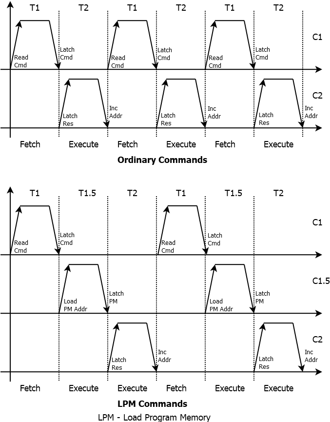
This command read (1 byte of) data from ROM, not RAM. And this command write data to register.
The data stores in the same ROM that stores the commands themselves.
Also you can use LPMW to read the whole 16 bit word from ROM and store data to register pair.
LD - LoaD data from memory
ST - STore data to memory
V - 0 for RAM and 1 for Video RAM
SRC - register to read
DST - register to write
EXT - register pair which store pointer to memory
D - Decrement pointer after use
U - Increment pointer after use
OFFSET4 - 4 bit integer offset (-8...+7)
(CPU will read/write memory with address ptr(EXT) + OFFSET4)
Examples:
LD R0, X    ; read memory data from X pointer into the R0 register
ST Y, R1    ; write data from R1 into memory with address from Y pointer
ST YI, R1   ; write data and increment Y pointer
ST YD, R1   ; write data and decrement Y pointer
ST Y+5, R1  ; write data into memory address Y+5
LDV R7, V   ; read data from Video RAM with address V and store it into R7 (R7:R6 pair)
LDV R7, V+1 ; **disabled** command, you can use displacement only with X, Y and SP pointersCALL - call a function by offset
AFCALL - call a function to an absolute address
RET - return to the address stored on the stack
RETI - return from interrupt to the address stored on the stack
JMP - go by offset
NOP - no operation (do nothing)
STOP - the processor will stop executing the program
JL, JE, JNE, JG, JZ, JNZ, JC, JNC, JHC, JNHC - conditional jump instructions
JL - jump if less
JE - jump if equal
JNE - jump if not equal
JG - jump if greater
JZ - jump if zero
JNZ - jump if not zero
JC - jump if carry
JNC - jump if not carry
JHC - jump if half carry
JNHC - jump if not half carry
| Qty | Value | Footprint | References |
|---|---|---|---|
| 11 | Conn_01x01_Male | Connector_PinHeader_2.54mm:PinHeader_1x01_P2.54mm_Vertical | J2, J7, J8, J9, J10, J11, J12, J13, J17, J18, J19 |
| 5 | 0.1uF | Capacitor_SMD:C_0805_2012Metric_Pad1.18x1.45mm_HandSolder | C1, C3, C4, C5, C6 |
| 3 | MountingHole | MountingHole:MountingHole_3.2mm_M3 | H1, H2, H3 |
| 2 | 10k | Resistor_SMD:R_0805_2012Metric_Pad1.20x1.40mm_HandSolder | R1, R2 |
| 2 | 74LS138 | Package_DIP:DIP-16_W7.62mm_Socket | U2, U4 |
| 2 | Conn_01x04_Male | Connector_PinHeader_2.54mm:PinHeader_1x04_P2.54mm_Vertical | J1, J16 |
| 2 | Conn_01x08_Male | Connector_PinHeader_2.54mm:PinHeader_1x08_P2.54mm_Vertical | J4, J5 |
| 1 | 1k | Resistor_SMD:R_0805_2012Metric_Pad1.20x1.40mm_HandSolder | R5 |
| 1 | 74HC00 | Package_DIP:DIP-14_W7.62mm_Socket | U6 |
| 1 | 74LS08 | Package_DIP:DIP-14_W7.62mm_Socket | U1 |
| 1 | 74LS139 | Package_DIP:DIP-16_W7.62mm_Socket | U3 |
| 1 | 74LS85 | Package_DIP:DIP-16_W7.62mm_Socket | U5 |
| 1 | Conn_01x02_Male | Connector_PinHeader_2.54mm:PinHeader_1x02_P2.54mm_Vertical | J6 |
| 1 | Conn_01x03_Male | Connector_PinHeader_2.54mm:PinHeader_1x03_P2.54mm_Vertical | J15 |
| 1 | Conn_01x05_Male | Connector_PinHeader_2.54mm:PinHeader_1x05_P2.54mm_Vertical | J3 |
| 1 | LED | LED_THT:LED_D5.0mm | D1 |
| 1 | Screw_Terminal_01x02 | TerminalBlock_Phoenix:TerminalBlock_Phoenix_MKDS-1,5-2_1x02_P5.00mm_Horizontal | J14 |


hanshuebner/cpc-floppy-controllers
MOVED to code.netzhansa.com/hanshuebner/cpc-floppy-controllers. This GitHub mirror is archived.


tergav17/Z80-MegaMapper
Z80 interposer board providing extended memory and I/O instruction mapping


TSJR/logic-analyzer
TTL logic analyzer built from 74xx logic and LED dot matrix display

crankery/crank68
One day I thought to myself I want to build a computer with the simplest 8 bit CPU I can think of". That CPU is the Motorola M6800 and this is the computer.


digilogistist/The-Open-Source-USB-NES-Project
USB-NES and NES-FASTGFX product engineering repository
It measures 78.7 × 50.8 mm and has 2 copper layers, 1.6 mm thick.
37 parts, built around the 74HC00D, 74LS139PC and 74LS85DC. The full list of its parts is on this page, with links to each part's symbol and footprint where PCBKit's library has them.
From the TheJustMoose/74HCPU repository on GitHub, at the commit this page was made from: the board is hard/!CMD_DEC/CMD_DEC/CMD_DEC.kicad_pcb. PCBKit opens the board in the browser, with nothing to install.
Its repository states no licence, so its author keeps all rights: ask TheJustMoose before reusing the design.