4 layers35 × 99.9 mm
Snips controller
thePunderWoman/SnipsControllers
The controllers built to work with Amidala
95 parts3GPL-2.0

 thePunderWoman/SnipsControllers3
The controllers built to work with Amidala
Snips controller is an open-source printed circuit board by thePunderWoman, from the thePunderWoman/SnipsControllers repository on GitHub, published under the GPL-2.0 licence. It is a 4-layer board of 30 × 70 mm with 94 parts on 56 nets, routed with 945 tracks and 127 vias.
It belongs with the ESP32 boards of this library.
A wireless handheld controller for R2-D2 droid operation, designed for use at public events and conventions. Communicates with the droid over Zigbee, in a packetized state-report architecture.
The electrical design is in Stackup KDL, using the pinned
Stackup library plus a local thumbstick model. The existing KiCad PCB is linked
through snips_controller.stackup_sch; sync it with the Stackup KiCad plugin. Run
stackup check PCB/v2.x/snips/stackup/board.kdl from the repository root before syncing.
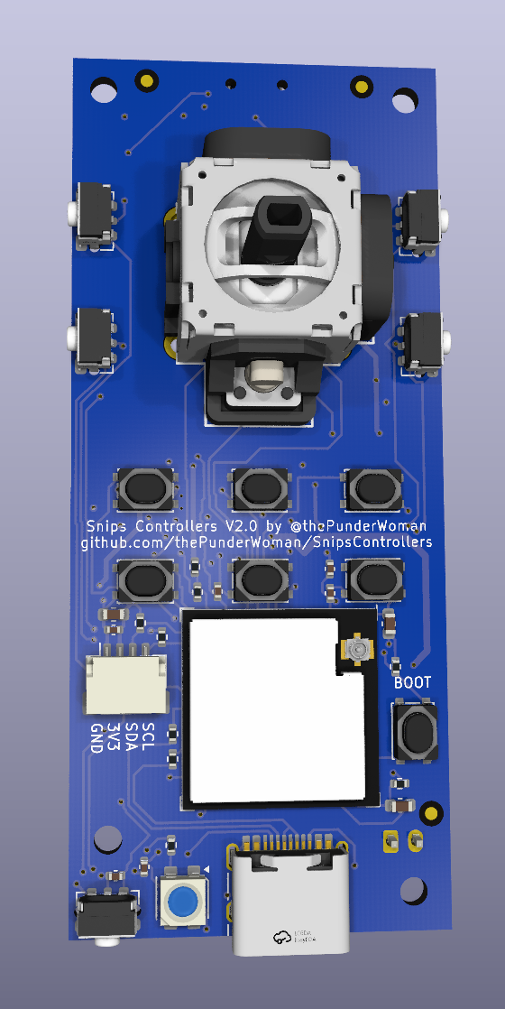
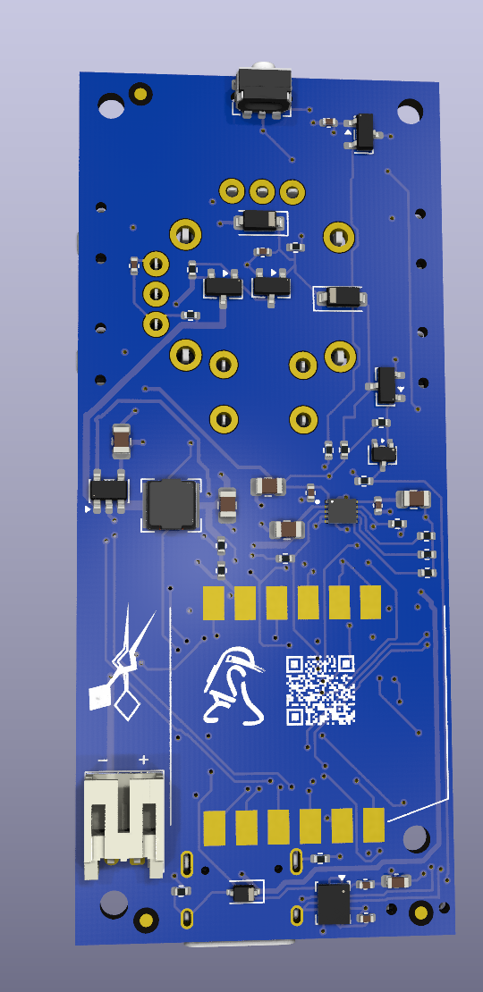
A STEP model of the assembled board is in step/v2.0/snips_controller.step.
70 x 30 mm, 4 layers: F.Cu signals, In1 solid 3V3, In2 solid GND, B.Cu signals. 1.6 mm thick. Routed, not yet fabricated.
GPIO_table.md explains. USB runs about 15 mm as a result, which is well within full-speed limits. Bluetooth and ESP-NOW work with no other radio.GPIO_table.md.GPIO_table.md.PWR_BTN_TRIGGER: the switch and PWR_LATCH_G node sit under the stick, turned 270 degrees, and the inverter sits beside the stick's lower pins. See diagrams/ for why they are arranged this way.C_DBNC1 by only about 0.15 mm. The carrier has a long shallow chamfer at that corner, which also clears a Ø4 post on the bottom.See GPIO_table.md for every module pin.
| Component | Part | Notes | Layout diagram |
|---|---|---|---|
| MCU and radio | Espressif ESP32-S3-MINI-1U-N8 | Wi-Fi, Bluetooth LE and ESP-NOW, 8 MB flash, 15.4 x 15.4 x 2.4 mm, external antenna | — |
| XBee (optional) | Digi XB3-24Z8UM on a castellated carrier | Zigbee 3.0, +19 dBm, U.FL. Hand-soldered to the underside | — |
| Display | SSD1306 1.3" OLED | 128x64, monochrome, I2C | — |
| Hall trigger | DRV5055A2QDBZR (SOT-23) | Ratiometric linear hall effect, 3.3V. On the bottom of the board under the trigger magnet; senses the field perpendicular to the board. Trigger calibration accepts either magnet polarity | — |
| Thumbstick | GuliKit hall effect module | Native 3.3V, analog X/Y + click | — |
| Macro and boot buttons | Alps SKRPABE010 | 4.2 x 3.2 x 2.5 mm SMD tact switch, 1.57 N, 0.2 mm travel, 100,000 cycles. Footprint checked against the Alps land drawing | — |
| RGB LED | SK6812MINI-HS | Status indicator; specified supply begins at 3.7 V, but board supplies 3.3 V | — |
| Charger | bq25185 | USB/DC input, power path, 4.2V/500mA | diagram |
| Buck | TLV62569 | 3.3V output, 2A | diagram |
| Battery | Single-cell pouch, 2-pin JST PH | Cell not chosen yet. Set R_ISET1 for it; 604 Ω charges at about 500 mA | — |
| Power switch | AO3401A + AO3400A | Soft latch, hybrid hardware+firmware | diagram |
Suggested top-copper floorplans for the three sheets with real layout
stakes — a switching regulator, a linear charger with a thermal pad, and
the soft latch that switches the buck's enable. Each is checked
against the actual component datasheet, not just the schematic. See
diagrams/README.md for the full list and how the
files are organized.
/Power_Buck/* nets in Stackup/Power_Charger/* nets in Stackup/Power_Control/* nets in Stackup| Component | Value | Notes |
|---|---|---|
| DRV5055 VCC | 100nF ceramic | |
| GuliKit VCC | 100nF ceramic | |
| SK6812 VCC | 100nF ceramic | Close to supply pin |
| ICM-42670-P | 100nF + 2.2µF on VDD, 10nF on VDDIO | Close to their pins |
| OLED connector | 1µF + 100nF ceramic | |
| bq25185 VIN | 10µF + 100nF ceramic | |
| bq25185 SYS | 10µF + 100nF ceramic | |
| bq25185 BAT | 10µF ceramic | |
| TLV62569 VIN | 10µF ceramic | |
| TLV62569 VOUT | 22µF ceramic | As on V1. TI specifies 10-47 µF |
| ESP32-S3-MINI-1U 3V3 | 10µF + 100nF + 39pF ceramic | As on V1 |
| ESP32-S3-MINI-1U EN | 1µF ceramic | With R_EN_PU1, per Espressif |
| XBee VCC | 10µF + 1µF + 47pF ceramic | On the carrier, per Digi 90001543 p.52 |
| Signal | Value | Notes |
|---|---|---|
| bq25185 STAT1/STAT2 | 10kΩ | Open drain, pulled up to 3V3 |
| bq25185 TS/MR | 10kΩ to GND | Required with no thermistor: floating means no charging |
| I2C SDA/SCL | 4.7kΩ | So the IMU works with no OLED attached |
| Boot button | 10kΩ to 3V3 | R_BOOT_PU1 |
| ESP32 EN | 10kΩ to 3V3 | R_EN_PU1 |
| USB D+/D- | 27Ω series | R_USB_DP1 and R_USB_DM1, as on V1 |
| Trigger output | 1kΩ + 100nF | R_TRIG1 and C_TRIG1, about 1.6 kHz. The DRV5055 must not see a capacitor without a resistor |
| SK6812 DIN | 470Ω | R_RGB1 |
No external parts. Every button wires to GND and a module GPIO, using the internal pull-ups; see GPIO_table.md.
The droids use XBee Zigbee 3.0, so the controller joins that network through the XBee on the carrier, over UART in API mode. Each droid has its own coordinator and PAN ID, and all coordinators share one AES key. Without the carrier the ESP32 can use Bluetooth or ESP-NOW.
Recommended bringup order:
PWR_HOLD reads high.PWR_EN and PWR_LATCH_G: the board must stay off every time, since the simulation's margin has not been measured.Firmware implements tiered power saving:
| Qty | Value | Footprint | References |
|---|---|---|---|
| 7 | 100nF 16V X7R ±10% | CL05B104KO5NNNC | Samsung | 0402 | Capacitor_SMD:C_0402_1005Metric | C_DBNC1, C_HALL1, C_OLED_2, C_RGB1, C_STICK1, C_SYS_2, C_VIN_2 |
| 7 | Tact switch 1.6N 100k cycles | SKRPABE010 | Alps | SMD 4.2x3.2x2.5mm | top actuated | SW_Alps_SKRP | SW_BOOT1, SW_MACRO1, SW_MACRO2, SW_MACRO3, SW_MACRO4, SW_MACRO5, SW_MACRO6 |
| 6 | Fiducial_1mm_Mask2mm | Fiducial:Fiducial_1mm_Mask2mm | FID1, FID2, FID3, FID4, FID5, FID6 |
| 6 | Side-push tact switch 1.6N 100k cycles | SKRTLAE010 | Alps | SMD 4.5x3.4x3.3mm | right-angle | Button_Switch_SMD:SW_Push_1P1T-MP_NO_Horizontal_Alps_SKRTLAE010 | SW_PWR1, SW_THR_DN1, SW_THR_UP1, SW_TRIG_DIG1, SW_VOL_DN1, SW_VOL_UP1 |
| 4 | 100nF 16V X7R ±10% | CL05B104KO5NNNC | Samsung | 0402 | C_0402_1005Metric | C_IMU_1, C_MCU_2, C_TRIG1, C_VSYS1 |
| 4 | 10kΩ ±1% 62.5mW | 0402WGF1002TCE | UNI-ROYAL | 0402 | Resistor_SMD:R_0402_1005Metric | R_BOOT_PU1, R_STAT1, R_STAT2, R_TS1 |
| 4 | 10µF 25V X5R ±10% | CL21A106KAYNNNE | Samsung | 0805 | Capacitor_SMD:C_0805_2012Metric | C_BAT1, C_BUCK_IN1, C_SYS_1, C_VIN_1 |
| 4 | MountingHole_2.2mm_M2_ISO14580 | MountingHole:MountingHole_2.2mm_M2_ISO14580 | MH1, MH2, MH3, MH4 |
| 3 | 100kΩ ±1% 62.5mW | 0402WGF1003TCE | UNI-ROYAL | 0402 | Resistor_SMD:R_0402_1005Metric | R_BTN_PU1, R_GATE1, R_VSYS2 |
| 3 | 1µF 50V X5R ±10% | CL10A105KB8NNNC | Samsung | 0603 | C_0603_1608Metric | C_EN1, C_LATCH_FB1, C_OLED_1 |
| 2 | 1N4148W switching diode 75V 150mA | 1N4148W | ST | SOD-123 | Diode_SMD:D_SOD-123 | D_OR1, D_OR2 |
| 2 | 220kΩ ±1% 62.5mW | 0402WGF2203TCE | UNI-ROYAL | 0402 | Resistor_SMD:R_0402_1005Metric | R_INV_BASE1, R_INV_PU1 |
| 2 | 27Ω ±1% 62.5mW | RC0402FR-0727RL | Yageo | 0402 | R_0402_1005Metric | R_USB_DM1, R_USB_DP1 |
| 2 | 4.7kΩ ±1% 62.5mW | 0402WGF4701TCE | UNI-ROYAL | 0402 | R_0402_1005Metric | R_I2C_SCL1, R_I2C_SDA1 |
| 2 | 5.1kΩ ±1% 62.5mW | 0402WGF5101TCE | UNI-ROYAL | 0402 | Resistor_SMD:R_0402_1005Metric | R_CC1, R_CC2 |
| 2 | LOGO | LOGO | LOGO1, LOGO2 |
| 1 | 1-cell Li-ion charger 1A | BQ25185DLHR | TI | WSON-10 | BQ25185DLHR:IC_BQ25185DLHR | U_CHG1 |
| 1 | 10kΩ ±1% 62.5mW | 0402WGF1002TCE | UNI-ROYAL | 0402 | R_0402_1005Metric | R_EN_PU1 |
| 1 | 10nF 50V X7R ±10% | CL05B103KB5NNNC | Samsung | 0402 | C_0402_1005Metric | C_IMU_3 |
| 1 | 10µF 10V X5R ±10% | CL10A106KP8NNNC | Samsung | 0603 | C_0603_1608Metric | C_MCU_1 |
| 1 | 18kΩ ±1% 62.5mW | RC0402FR-0718KL | Yageo | 0402 | Resistor_SMD:R_0402_1005Metric | R_VSET1 |
| 1 | 1MΩ ±1% 62.5mW | 0402WGF1004TCE | UNI-ROYAL | 0402 | Resistor_SMD:R_0402_1005Metric | R_LATCH_G1 |
| 1 | 1kΩ ±1% 62.5mW | 0402WGF1001TCE | UNI-ROYAL | 0402 | R_0402_1005Metric | R_TRIG1 |
| 1 | 1µF 6.3V X5R ±10% | CL05A105KQ5NNNC | Samsung | 0402 | Capacitor_SMD:C_0402_1005Metric | C_LATCH_G1 |
| 1 | 2.2µF 10V X7R ±10% | CL10B225KP8NNNC | Samsung | 0603 | C_0603_1608Metric | C_IMU_2 |
| 1 | 2.2µH ±20% 2.9A 44mΩ power inductor | SRN4018-2R2M | Bourns | SMD 4x4mm | Inductor_SMD:L_Bourns-SRN4018 | L_BUCK1 |
| 1 | 200kΩ ±1% 62.5mW | 0402WGF2003TCE | UNI-ROYAL | 0402 | Resistor_SMD:R_0402_1005Metric | R_VSYS1 |
| 1 | 22kΩ ±1% 62.5mW | 0402WGF2202TCE | UNI-ROYAL | 0402 | Resistor_SMD:R_0402_1005Metric | R_PWR_EN_PD1 |
| 1 | 22µF 25V X5R ±20% | CL21A226MAQNNNE | Samsung | 0805 | Capacitor_SMD:C_0805_2012Metric | C_BUCK_OUT1 |
| 1 | 255kΩ ±1% 62.5mW | RC0402FR-07255KL | Yageo | 0402 | Resistor_SMD:R_0402_1005Metric | R_FB1 |
| 1 | 39pF 50V NP0 ±5% | CC0402JRNPO9BN390 | Yageo | 0402 | C_0402_1005Metric | C_MCU_3 |
| 1 | 470Ω ±1% 62.5mW | 0402WGF4700TCE | UNI-ROYAL | 0402 | Resistor_SMD:R_0402_1005Metric | R_RGB1 |
| 1 | 56.2kΩ ±1% 62.5mW | RC0402FR-0756K2L | Yageo | 0402 | Resistor_SMD:R_0402_1005Metric | R_FB2 |
| 1 | 6-axis IMU | ICM-42670-P | TDK InvenSense | LGA-14 2.5x3mm | LGA-14_3x2.5mm_P0.5mm_LayoutBorder3x4y | U_IMU1 |
| 1 | 604Ω ±1% 62.5mW | AC0402FR-07604RL | Yageo | 0402 | Resistor_SMD:R_0402_1005Metric | R_ISET1 |
| 1 | Addressable RGB LED | SK6812MINI-HS | OPSCO | 3.5x3.5mm SMD | top-mount lens up | SK6812MINI-HS-012 | D_RGB1 |
| 1 | Adjustable buck converter 2A | TLV62569DBVR | TI | SOT-23-5 | Package_TO_SOT_SMD:SOT-23-5 | U_BUCK1 |
| 1 | Hall thumbstick | GuliKit_Thumbstick | GuliKit | Through-hole | DNP - hand-fitted - do not assemble | SnipsControllers_Custom:GuliKit_HallStick | J_STICK1 |
| 1 | JST PH 2-pin 2mm | S2B-PH-K(LF)(SN) | JST | Through-hole | RIGHT-ANGLE HORIZONTAL not vertical | Connector_JST:JST_PH_S2B-PH-K_1x02_P2.00mm_Horizontal | BT1 |
| 1 | JST SH 4-pin 1mm Qwiic | SM04B-SRSS-TB(LF)(SN) | JST | SMD | side entry right-angle | Connector_JST:JST_SH_SM04B-SRSS-TB_1x04-1MP_P1.00mm_Horizontal | U_OLED1 |
| 1 | LOGO | R2Builders:R2Builders | LOGO3 |
| 1 | Linear hall sensor A2 ±42mT | DRV5055A2QDBZR | TI | SOT-23 | SOT-23 | U_HALL1 |
| 1 | N-channel MOSFET 30V 5.7A | AO3400A | AOS | SOT-23 | Package_TO_SOT_SMD:SOT-23 | Q_LATCH1 |
| 1 | NPN transistor 40V 200mA hFE 100-300 | MMBT3904(RANGE:100-300) | JCET | SOT-23 | Package_TO_SOT_SMD:SOT-23 | Q_INV1 |
| 1 | P-channel MOSFET 30V 4A | AO3401A | AOS | SOT-23 | Package_TO_SOT_SMD:SOT-23 | Q_PWR1 |
| 1 | Schottky diode 30V 200mA | BAT54W-7-F | Diodes Inc | SOT-323 | Package_TO_SOT_SMD:SOT-323_SC-70 | D_INV_ISO1 |
| 1 | TVS diode 5V bidirectional | TPPESD5V0S1BA | TECH PUBLIC | SOD-323 | Diode_SMD:D_SOD-323 | D_VBUS_TVS1 |
| 1 | USB-C receptacle 16-pin | TYPE-C-31-M-12 | Hroparts Elec | SMD with through-hole shell tabs | right-angle | Connector_USB:USB_C_Receptacle_HRO_TYPE-C-31-M-12 | J_USB1 |
| 1 | Wi-Fi BLE module 8MB flash no PSRAM | ESP32-S3-MINI-1U-N8 | Espressif | SMD module 15.4x15.4mm | N8 variant with external antenna connector | ESP32-S3-MINI-1U | U_MCU1 |
| 1 | XBee carrier pads no part | Snips XBee carrier | Snips Controllers | Copper pads only | DNP - hand-soldered daughter board - do not assemble | XBee_Carrier_Castellated | U_XBEE1 |
thePunderWoman/SnipsControllers
The controllers built to work with Amidala

thePunderWoman/SnipsControllers
The controllers built to work with Amidala


will127534/OneInchEye
A One Inch CMOS sensor (IMX283) camera board designed for Raspberry Pi


endofexclusive/greta
GRETA expansion board for the Amiga 500 computer with Fast RAM, microSD mass storage and Ethernet controller, powered by FPGA technology.


Gmanmodz/RVL-Power-Management-System
A complete battery management and custom regulator system for a Wii portable


netik/dc25_spqr_badge
KiCad files and all component files to manufacture the IDES OF DEF CON Badge, an Unofficial Electronic Badge.
It measures 30 × 70 mm and has 4 copper layers, 1.6 mm thick.
94 parts. The full list of its parts is on this page, with links to each part's symbol and footprint where PCBKit's library has them.
From the thePunderWoman/SnipsControllers repository on GitHub, at the commit this page was made from: the board is PCB/v2.x/snips/snips_controller.kicad_pcb. PCBKit opens the board in the browser, with nothing to install.
Its repository publishes it under the GPL-2.0 licence: you may reuse it on that licence's terms (keep the author's notice, and for a copyleft licence share your changes alike).