4 layers30 × 70 mm
Snips controller
thePunderWoman/SnipsControllers
The controllers built to work with Amidala
94 parts3GPL-2.0
 thePunderWoman/SnipsControllers3
The controllers built to work with Amidala
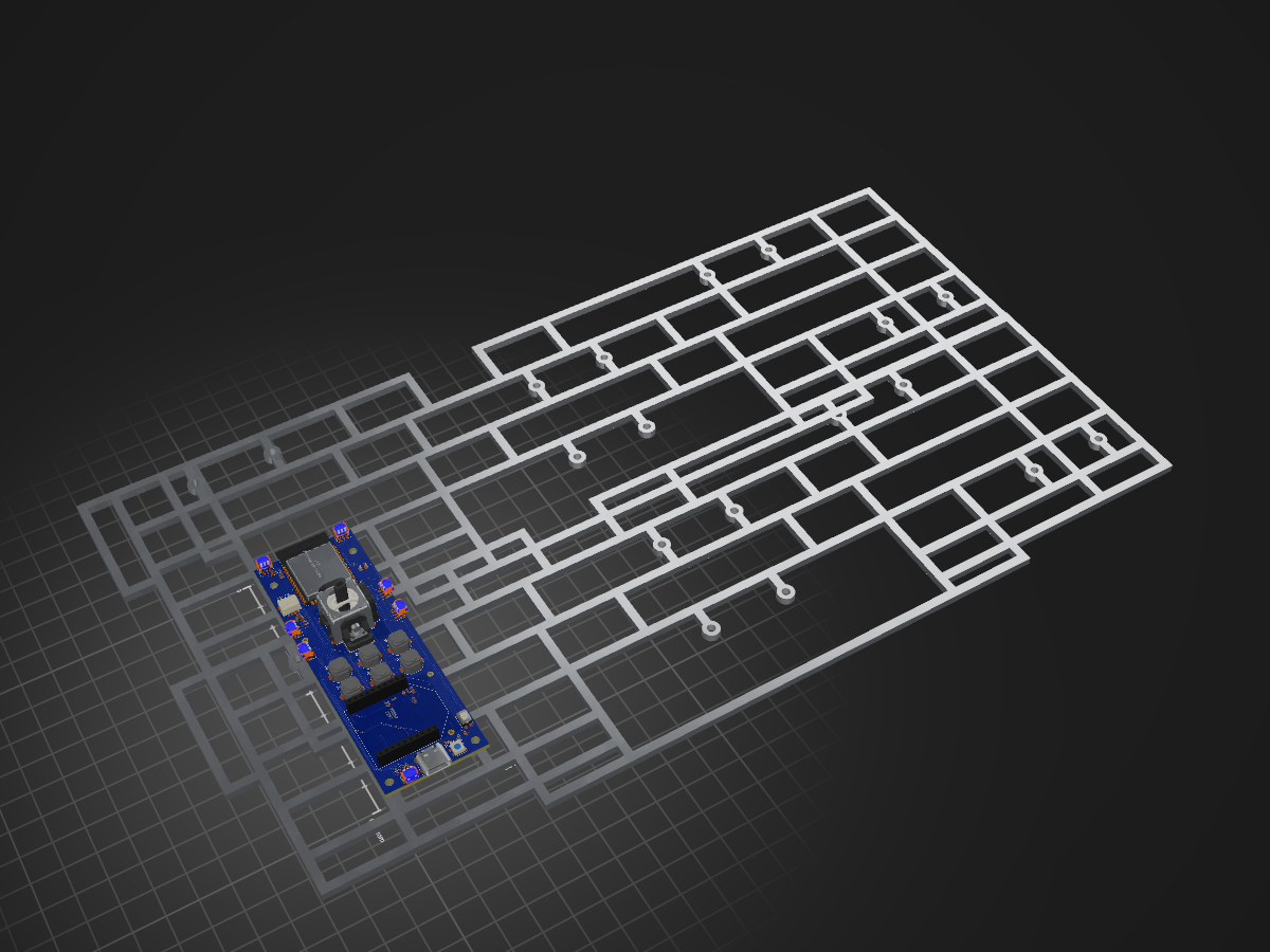
Snips controller is an open-source printed circuit board by thePunderWoman, from the thePunderWoman/SnipsControllers repository on GitHub, published under the GPL-2.0 licence. It is a 4-layer board of 35 × 99.9 mm with 95 parts on 57 nets, routed with 1,121 tracks and 130 vias.
It is built around the ESP32-S3-WROOM-1-N8, TLV62569DBVR-TP and SKRTLAE010, with the 1N4148W, AO3400A and AO3401A among its other parts. It belongs with the ESP32 boards of this library.


A wireless handheld controller for R2-D2 droid operation, designed for use at public events and conventions. Communicates with the droid over Zigbee, in a packetized state-report architecture.
The electrical design is in Stackup KDL, using the pinned
Stackup library plus a local thumbstick model. The existing KiCad PCB is linked
through snips_controller.stackup_sch; sync it with the Stackup KiCad plugin. Run
stackup check PCB/v2.x/snips/stackup/board.kdl from the repository root before syncing.
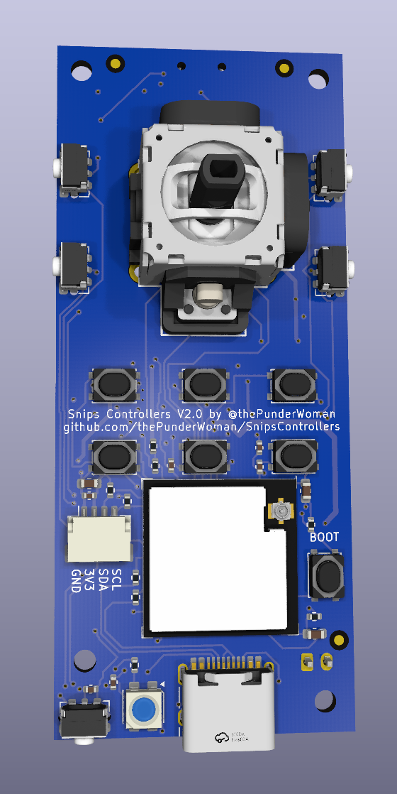
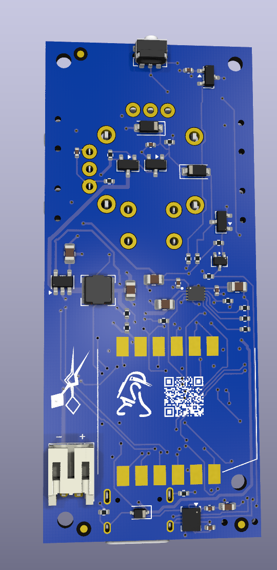
A STEP model of the assembled board is in step/v2.0/snips_controller.step.
70 x 30 mm, 4 layers: F.Cu signals, In1 solid 3V3, In2 solid GND, B.Cu signals. 1.6 mm thick. Routed, not yet fabricated.
GPIO_table.md explains. USB runs about 15 mm as a result, which is well within full-speed limits. Bluetooth and ESP-NOW work with no other radio.GPIO_table.md.GPIO_table.md.PWR_BTN_TRIGGER: the switch and PWR_LATCH_G node sit under the stick, turned 270 degrees, and the inverter sits beside the stick's lower pins. See diagrams/ for why they are arranged this way.C_DBNC1 by only about 0.15 mm. The carrier has a long shallow chamfer at that corner, which also clears a Ø4 post on the bottom.See GPIO_table.md for every module pin.
| Component | Part | Notes | Layout diagram |
|---|---|---|---|
| MCU and radio | Espressif ESP32-S3-MINI-1U-N8 | Wi-Fi, Bluetooth LE and ESP-NOW, 8 MB flash, 15.4 x 15.4 x 2.4 mm, external antenna | — |
| XBee (optional) | Digi XB3-24Z8UM on a castellated carrier | Zigbee 3.0, +19 dBm, U.FL. Hand-soldered to the underside | — |
| Display | SSD1306 1.3" OLED | 128x64, monochrome, I2C | — |
| Hall trigger | DRV5055A2QDBZR (SOT-23) | Ratiometric linear hall effect, 3.3V. On the bottom of the board under the trigger magnet; senses the field perpendicular to the board. Trigger calibration accepts either magnet polarity | — |
| Thumbstick | GuliKit hall effect module | Native 3.3V, analog X/Y + click | — |
| Macro and boot buttons | Alps SKRPABE010 | 4.2 x 3.2 x 2.5 mm SMD tact switch, 1.57 N, 0.2 mm travel, 100,000 cycles. Footprint checked against the Alps land drawing | — |
| RGB LED | SK6812MINI-HS | Status indicator; specified supply begins at 3.7 V, but board supplies 3.3 V | — |
| Charger | bq25185 | USB/DC input, power path, 4.2V/500mA | diagram |
| Buck | TLV62569 | 3.3V output, 2A | diagram |
| Battery | Single-cell pouch, 2-pin JST PH | Cell not chosen yet. Set R_ISET1 for it; 604 Ω charges at about 500 mA | — |
| Power switch | AO3401A + AO3400A | Soft latch, hybrid hardware+firmware | diagram |
Suggested top-copper floorplans for the three sheets with real layout
stakes — a switching regulator, a linear charger with a thermal pad, and
the soft latch that switches the buck's enable. Each is checked
against the actual component datasheet, not just the schematic. See
diagrams/README.md for the full list and how the
files are organized.
/Power_Buck/* nets in Stackup/Power_Charger/* nets in Stackup/Power_Control/* nets in Stackup| Component | Value | Notes |
|---|---|---|
| DRV5055 VCC | 100nF ceramic | |
| GuliKit VCC | 100nF ceramic | |
| SK6812 VCC | 100nF ceramic | Close to supply pin |
| ICM-42670-P | 100nF + 2.2µF on VDD, 10nF on VDDIO | Close to their pins |
| OLED connector | 1µF + 100nF ceramic | |
| bq25185 VIN | 10µF + 100nF ceramic | |
| bq25185 SYS | 10µF + 100nF ceramic | |
| bq25185 BAT | 10µF ceramic | |
| TLV62569 VIN | 10µF ceramic | |
| TLV62569 VOUT | 22µF ceramic | As on V1. TI specifies 10-47 µF |
| ESP32-S3-MINI-1U 3V3 | 10µF + 100nF + 39pF ceramic | As on V1 |
| ESP32-S3-MINI-1U EN | 1µF ceramic | With R_EN_PU1, per Espressif |
| XBee VCC | 10µF + 1µF + 47pF ceramic | On the carrier, per Digi 90001543 p.52 |
| Signal | Value | Notes |
|---|---|---|
| bq25185 STAT1/STAT2 | 10kΩ | Open drain, pulled up to 3V3 |
| bq25185 TS/MR | 10kΩ to GND | Required with no thermistor: floating means no charging |
| I2C SDA/SCL | 4.7kΩ | So the IMU works with no OLED attached |
| Boot button | 10kΩ to 3V3 | R_BOOT_PU1 |
| ESP32 EN | 10kΩ to 3V3 | R_EN_PU1 |
| USB D+/D- | 27Ω series | R_USB_DP1 and R_USB_DM1, as on V1 |
| Trigger output | 1kΩ + 100nF | R_TRIG1 and C_TRIG1, about 1.6 kHz. The DRV5055 must not see a capacitor without a resistor |
| SK6812 DIN | 470Ω | R_RGB1 |
No external parts. Every button wires to GND and a module GPIO, using the internal pull-ups; see GPIO_table.md.
The droids use XBee Zigbee 3.0, so the controller joins that network through the XBee on the carrier, over UART in API mode. Each droid has its own coordinator and PAN ID, and all coordinators share one AES key. Without the carrier the ESP32 can use Bluetooth or ESP-NOW.
Recommended bringup order:
PWR_HOLD reads high.PWR_EN and PWR_LATCH_G: the board must stay off every time, since the simulation's margin has not been measured.Firmware implements tiered power saving:
| Qty | Value | Footprint | References |
|---|---|---|---|
| 11 | 100nF | Capacitor_SMD:C_0402_1005Metric | C_3V3_2, C_DBNC1, C_HALL1, C_LATCH_G1, C_OLED_2, C_RGB1, C_STICK1, C_SYS_2, C_VIN_2, C_XBEE_RC1, C_XBEE_VCC1 |
| 7 | 10kΩ | Resistor_SMD:R_0402_1005Metric | R_BOOT_PU1, R_EN_PU1, R_STAT1, R_STAT2, R_TS1, R_XBEE_ATTN_PU1, R_XBEE_RST1 |
| 7 | SKRTLAE010 | Button_Switch_SMD:SW_Push_1P1T-MP_NO_Horizontal_Alps_SKRTLAE010 | SW_PWR1, SW_THR_DN1, SW_THR_UP1, SW_TRIG_DIG1, SW_TRIG_DIG2, SW_VOL_DN1, SW_VOL_UP1 |
| 6 | 100kΩ | Resistor_SMD:R_0402_1005Metric | R_BTN_PU1, R_GATE1, R_INV_BASE1, R_INV_PU1, R_PWR_EN_PD1, R_VSYS2 |
| 6 | 6x6x5mm SMD Tactile | Button_Switch_SMD:SW_Push_1TS009xxxx-xxxx-xxxx_6x6x5mm | SW_MACRO1, SW_MACRO2, SW_MACRO3, SW_MACRO4, SW_MACRO5, SW_MACRO6 |
| 5 | 10µF | Capacitor_SMD:C_0805_2012Metric | C_BAT1, C_BUCK_IN1, C_OLED_1, C_SYS_1, C_VIN_1 |
| 5 | Fiducial_1mm_Mask2mm | Fiducial:Fiducial_1mm_Mask2mm | FID1, FID2, FID3, FID4, FID5 |
| 4 | MountingHole_2.7mm_M2.5 | MountingHole:MountingHole_2.7mm_M2.5 | MH1, MH2, MH3, MH4 |
| 2 | 10µF | Capacitor_SMD:C_0603_1608Metric | C_3V3_1, C_XBEE_VCC4 |
| 2 | 1N4148W | Diode_SMD:D_SOD-123 | D_OR1, D_OR2 |
| 2 | 27Ω | Resistor_SMD:R_0402_1005Metric | R_USB_DM1, R_USB_DP1 |
| 2 | 5.1kΩ | Resistor_SMD:R_0402_1005Metric | R_CC1, R_CC2 |
| 2 | LOGO | LOGO | LOGO1, LOGO2 |
| 1 | 100nF | C_0402_1005Metric | C_IMU_1 |
| 1 | 100Ω | Resistor_SMD:R_0402_1005Metric | R_XBEE_RC1 |
| 1 | 10nF | C_0402_1005Metric | C_IMU_3 |
| 1 | 18kΩ | Resistor_SMD:R_0402_1005Metric | R_VSET1 |
| 1 | 1MΩ | Resistor_SMD:R_0402_1005Metric | R_LATCH_G1 |
| 1 | 1µF | Capacitor_SMD:C_0603_1608Metric | C_XBEE_VCC2 |
| 1 | 2.2µF | C_0603_1608Metric | C_IMU_2 |
| 1 | 2.2µH | Inductor_SMD:L_Bourns-SRN4018 | L_BUCK1 |
| 1 | 200kΩ | Resistor_SMD:R_0402_1005Metric | R_VSYS1 |
| 1 | 22µF | Capacitor_SMD:C_0805_2012Metric | C_BUCK_OUT1 |
| 1 | 255kΩ | Resistor_SMD:R_0402_1005Metric | R_FB1 |
| 1 | 39pF | Capacitor_SMD:C_0402_1005Metric | C_3V3_3 |
| 1 | 470Ω | Resistor_SMD:R_0402_1005Metric | R_RGB1 |
| 1 | 47pF | Capacitor_SMD:C_0402_1005Metric | C_XBEE_VCC3 |
| 1 | 56.2kΩ | Resistor_SMD:R_0402_1005Metric | R_FB2 |
| 1 | 604Ω | Resistor_SMD:R_0402_1005Metric | R_ISET1 |
| 1 | AO3400A | Package_TO_SOT_SMD:SOT-23 | Q_LATCH1 |
| 1 | AO3401A | Package_TO_SOT_SMD:SOT-23 | Q_PWR1 |
| 1 | BAT54W-7-F | Package_TO_SOT_SMD:SOT-323_SC-70 | D_INV_ISO1 |
| 1 | BQ25185DLHR | BQ25185DLHR:IC_BQ25185DLHR | U_CHG1 |
| 1 | DRV5055A2QDBZR | SOT-23 | U_HALL1 |
| 1 | ESP32-S3-WROOM-1-N8 | Espressif:ESP32-S3-WROOM-1 | U_MCU1 |
| 1 | GuliKit_Thumbstick | SnipsControllers_Custom:GuliKit_HallStick | J_STICK1 |
| 1 | ICM-42670-P | LGA-14_3x2.5mm_P0.5mm_LayoutBorder3x4y | U_IMU1 |
| 1 | LOGO | R2Builders:R2Builders | LOGO3 |
| 1 | MMBT3904(RANGE:100-300) | Package_TO_SOT_SMD:SOT-23 | Q_INV1 |
| 1 | PH 2-pin battery RIGHT-ANGLE HORIZONTAL | Connector_JST:JST_PH_S2B-PH-K_1x02_P2.00mm_Horizontal | BT1 |
| 1 | Panasonic_EVQP2 | Button_Switch_SMD:SW_SPST_EVQP2_ShortPushTravel_H2.1mm | SW_BOOT1 |
| 1 | Qwiic connector | Connector_JST:JST_SH_SM04B-SRSS-TB_1x04-1MP_P1.00mm_Horizontal | U_OLED1 |
| 1 | SK6812MINI-HS-012 | SK6812MINI-HS-012 | D_RGB1 |
| 1 | TLV62569DBVR | Package_TO_SOT_SMD:SOT-23-5 | U_BUCK1 |
| 1 | TPPESD5V0S1BA | Diode_SMD:D_SOD-323 | D_VBUS_TVS1 |
| 1 | USB-C | Connector_USB:USB_C_Receptacle_HRO_TYPE-C-31-M-12 | J_USB1 |
| 1 | XBee3 | Xbee3:XB324Z8UTJ | U_XBEE1 |
thePunderWoman/SnipsControllers
The controllers built to work with Amidala

thePunderWoman/SnipsControllers
The controllers built to work with Amidala


Andreuxxx1977/esp32-p4
An open-hardware, actively cooled ESP32-P4 board for heavy multimedia work: a 2-lane MIPI camera, a 2-lane MIPI display, USB 2.0 High-Speed, 10/100 Ethernet, UHS-I microSD, 32 MB flash and 32 MB PSRAM.

Serhio4522/SEM_hitachi-
Digitization of a Hitachi scanning electron microscope (SEM) — hardware design, FPGA firmware, and analog frontend schematics.

windmoondreamer/pairing-voice-cube
아이가 목소리를 녹음하고, 부모가 버튼을 눌러 재생하는 장치의 회로기판 프로젝트. 80mm 큐브 케이스 · 최대 45초 녹음 · 내장 플래시 · 배터리 구동.


Alacrity-Education/AirBoxV2
The AirBox V2 Station is an open source air quality monitoring station based on the Sensirion SEN66 sensor. It measures particulate matter, CO2, VOC and NOx, runs on a solar charged lithium cell, and reports over Wi-Fi.
It measures 35 × 99.9 mm and has 4 copper layers, 1.6 mm thick.
95 parts, built around the ESP32-S3-WROOM-1-N8, TLV62569DBVR-TP, SKRTLAE010 and 1N4148W. The full list of its parts is on this page, with links to each part's symbol and footprint where PCBKit's library has them.
From the thePunderWoman/SnipsControllers repository on GitHub, at the commit this page was made from: the board is PCB/v1.x/snips_controller.kicad_pcb. PCBKit opens the board in the browser, with nothing to install.
Its repository publishes it under the GPL-2.0 licence: you may reuse it on that licence's terms (keep the author's notice, and for a copyleft licence share your changes alike).