

2 layers135.9 × 89.5 mm
Right
TeXitoi/keyseebee
KeySeeBee is a split ergo keyboard. It is only 2 PCB (so the name) with (almost) only SMD components on it. It's only a keyboard, no LED, no display, nothing more than keys and USB.
61 parts348MIT

KeySeeBee is a split ergo keyboard. It is only 2 PCB (so the name) with (almost) only SMD components on it. It's only a keyboard, no LED, no display, nothing more than keys and USB.
Left is an open-source printed circuit board by TeXitoi, from the TeXitoi/keyseebee repository on GitHub, published under the MIT licence. It is a 2-layer board of 135.9 × 89.5 mm with 61 parts on 68 nets, routed with 686 tracks and 33 vias.
It is built around the 1N4148WS. Its parts include 24 switches, 22 diodes, 7 capacitors, 3 resistors and 3 connectors. It belongs with the keyboards and input and lEDs and displays boards and the STM32 boards of this library.
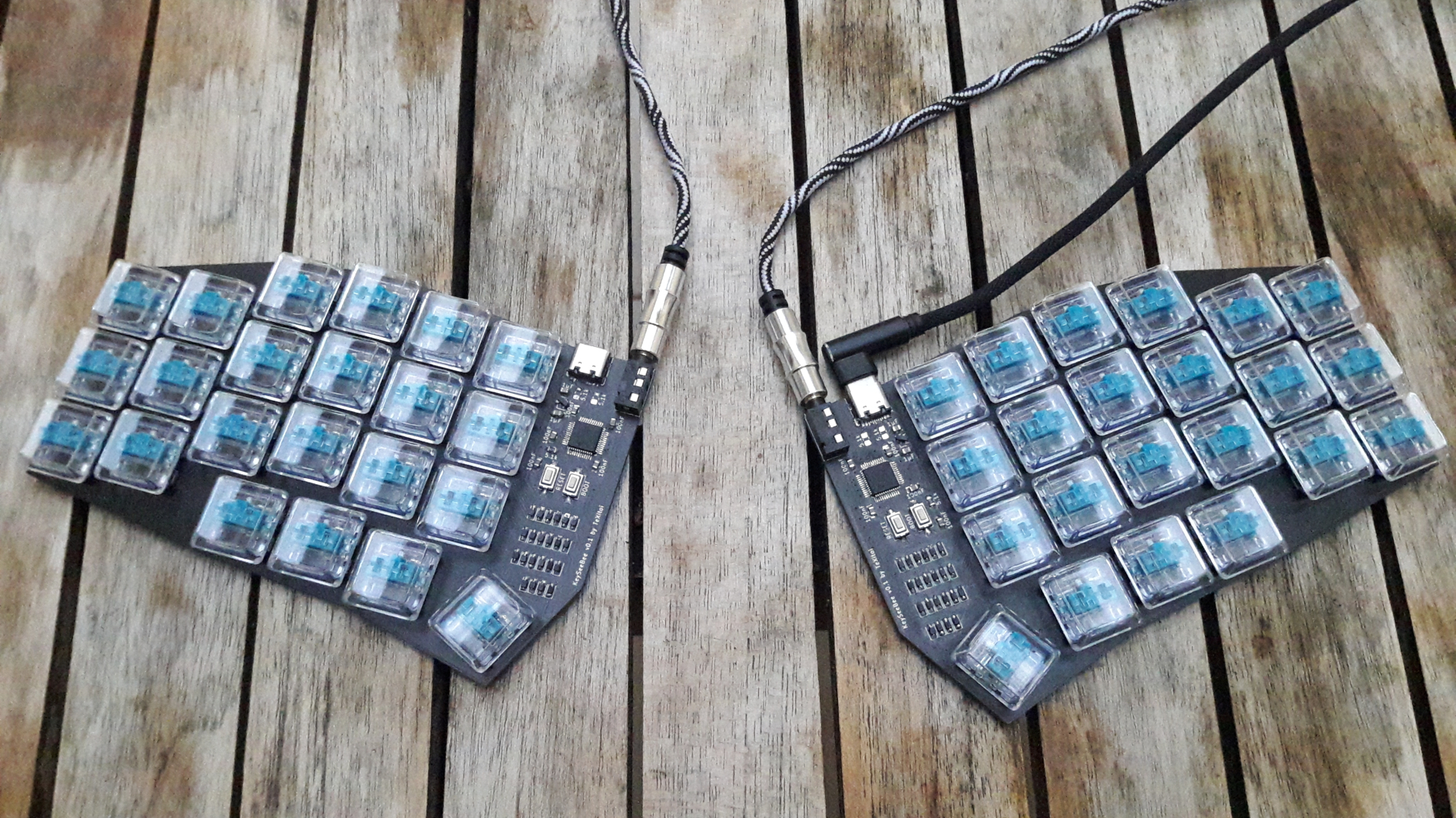
KeySeeBee is a split ergo keyboard. It is only 2 PCB (so the name) with (almost) only SMD components on it. It's only a keyboard, no LED, no display, nothing more than keys and USB.
The firmware is Keyberon, a pure rust firmware.
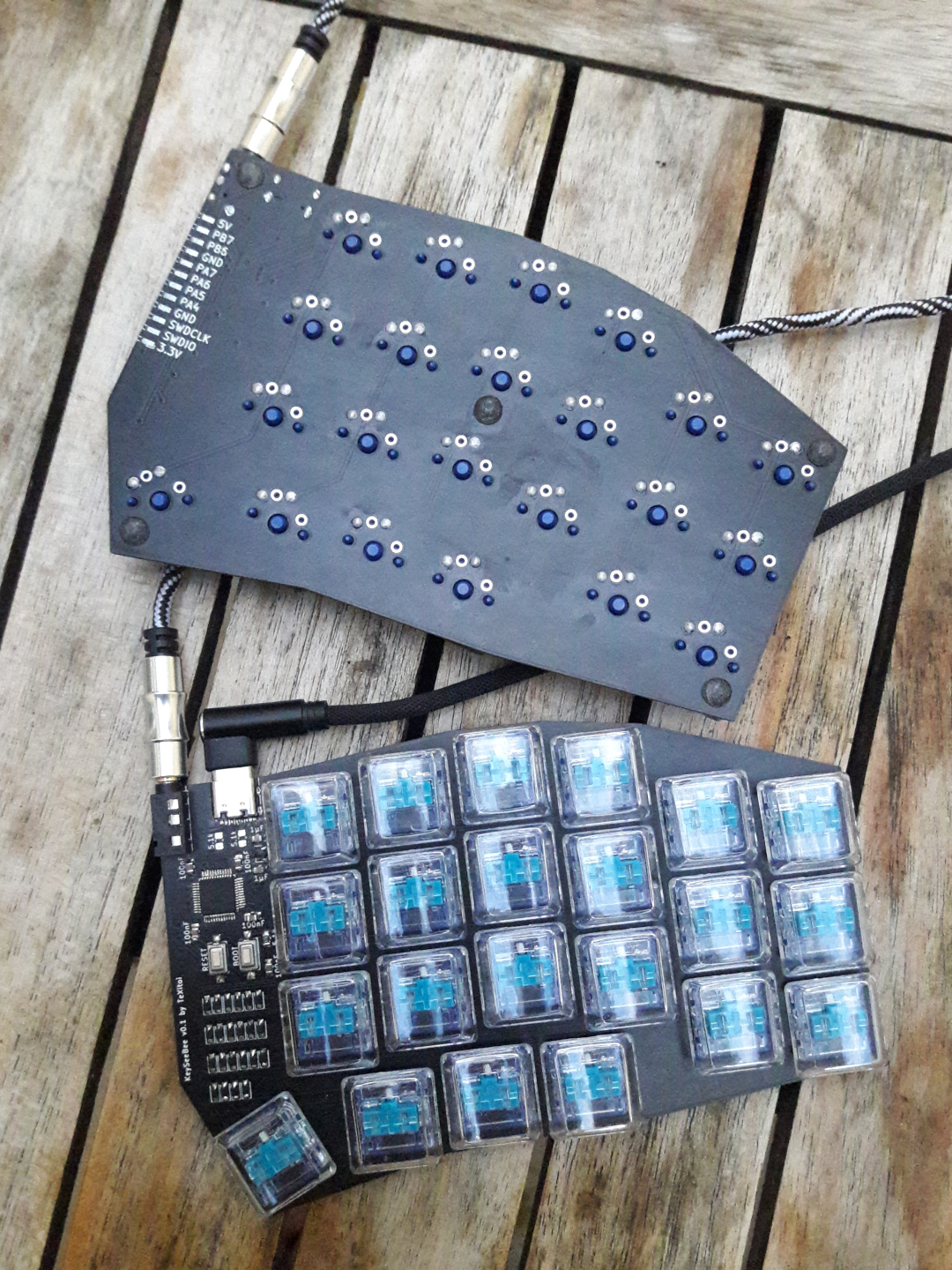
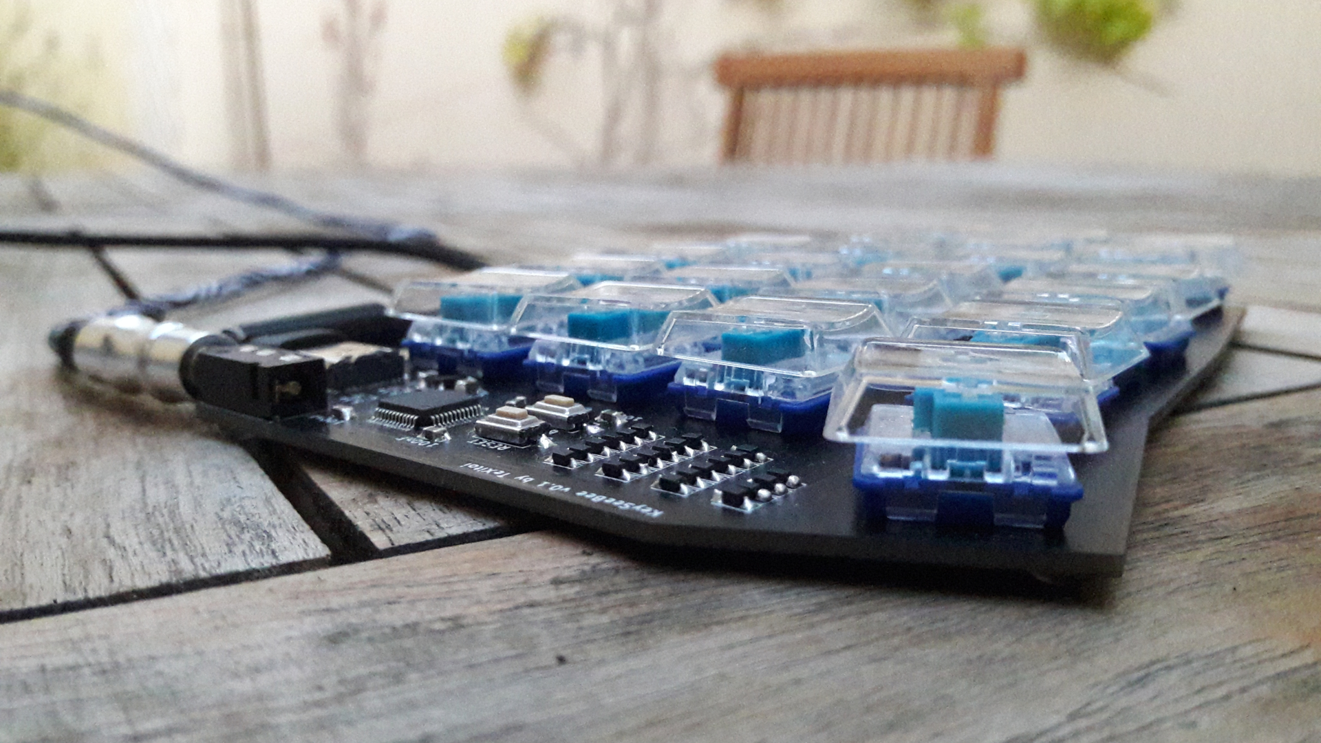
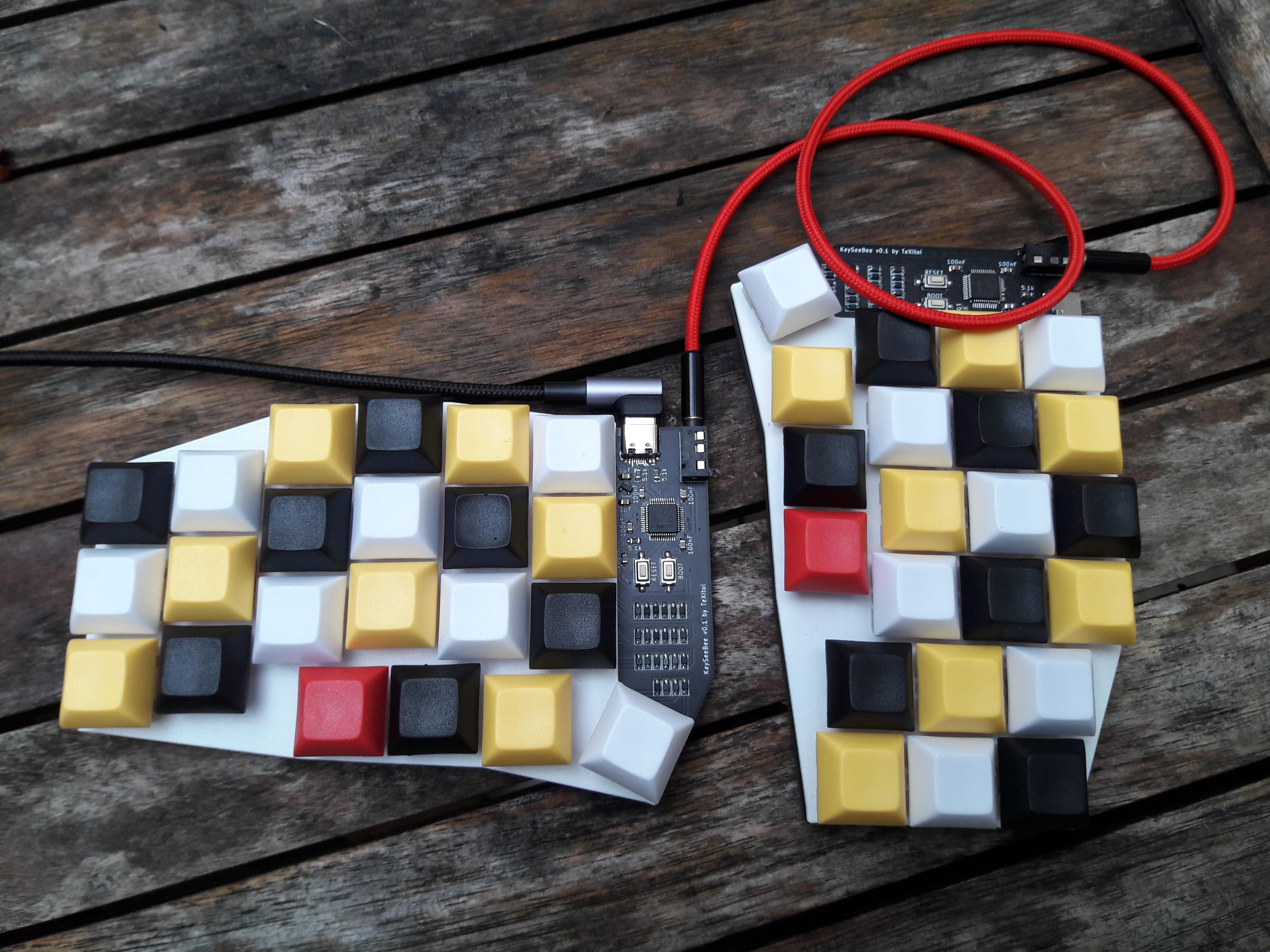
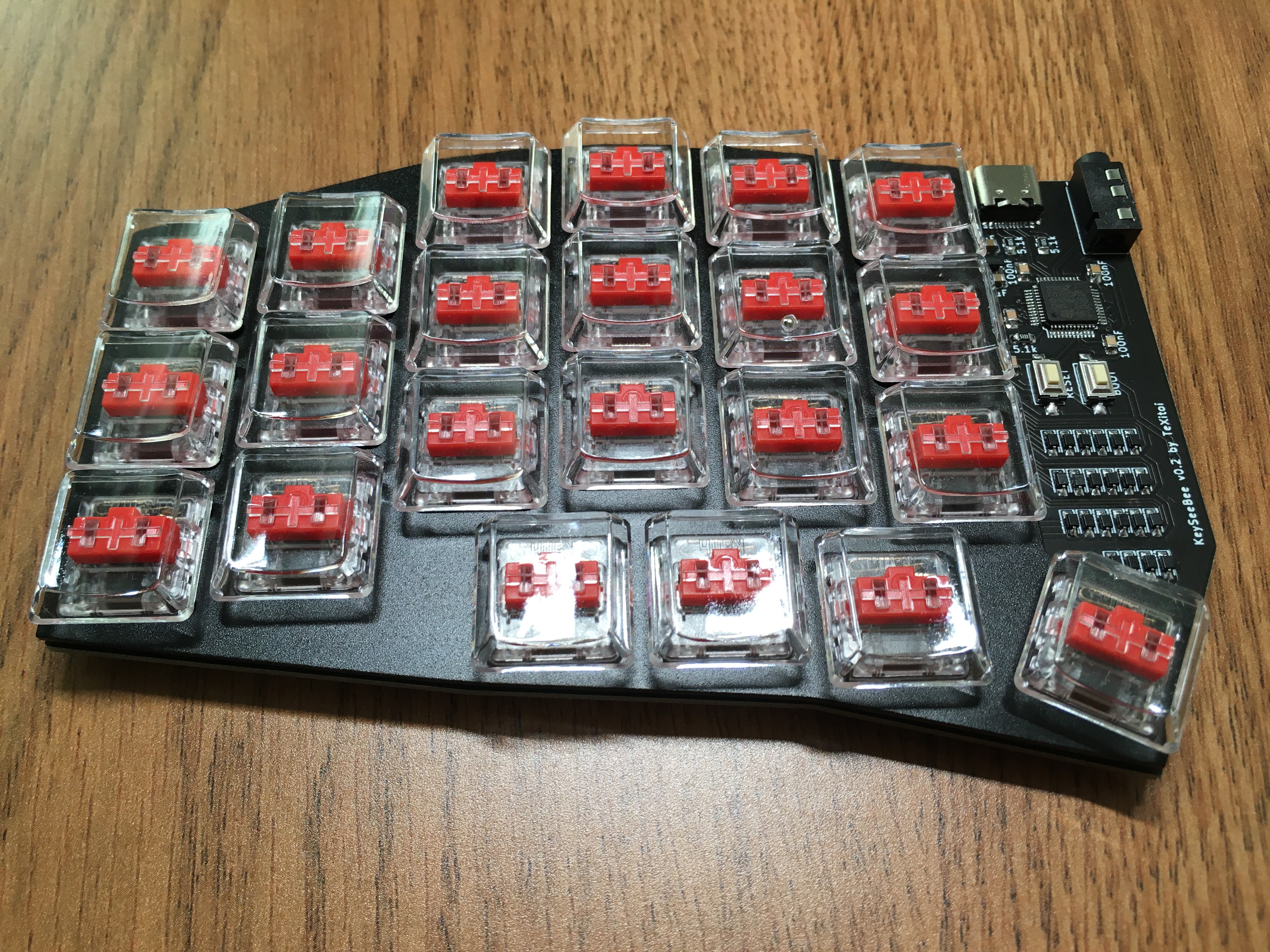
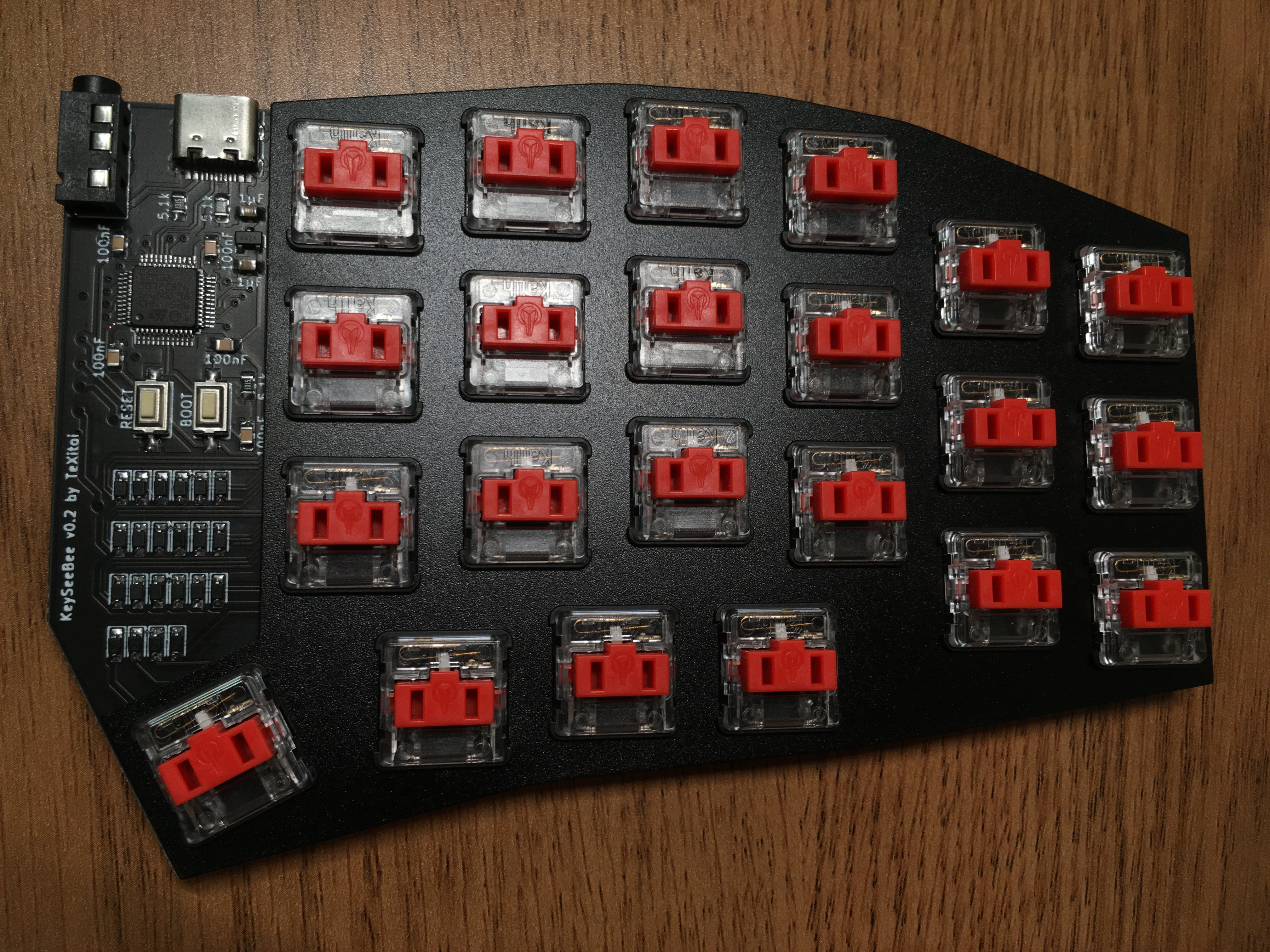
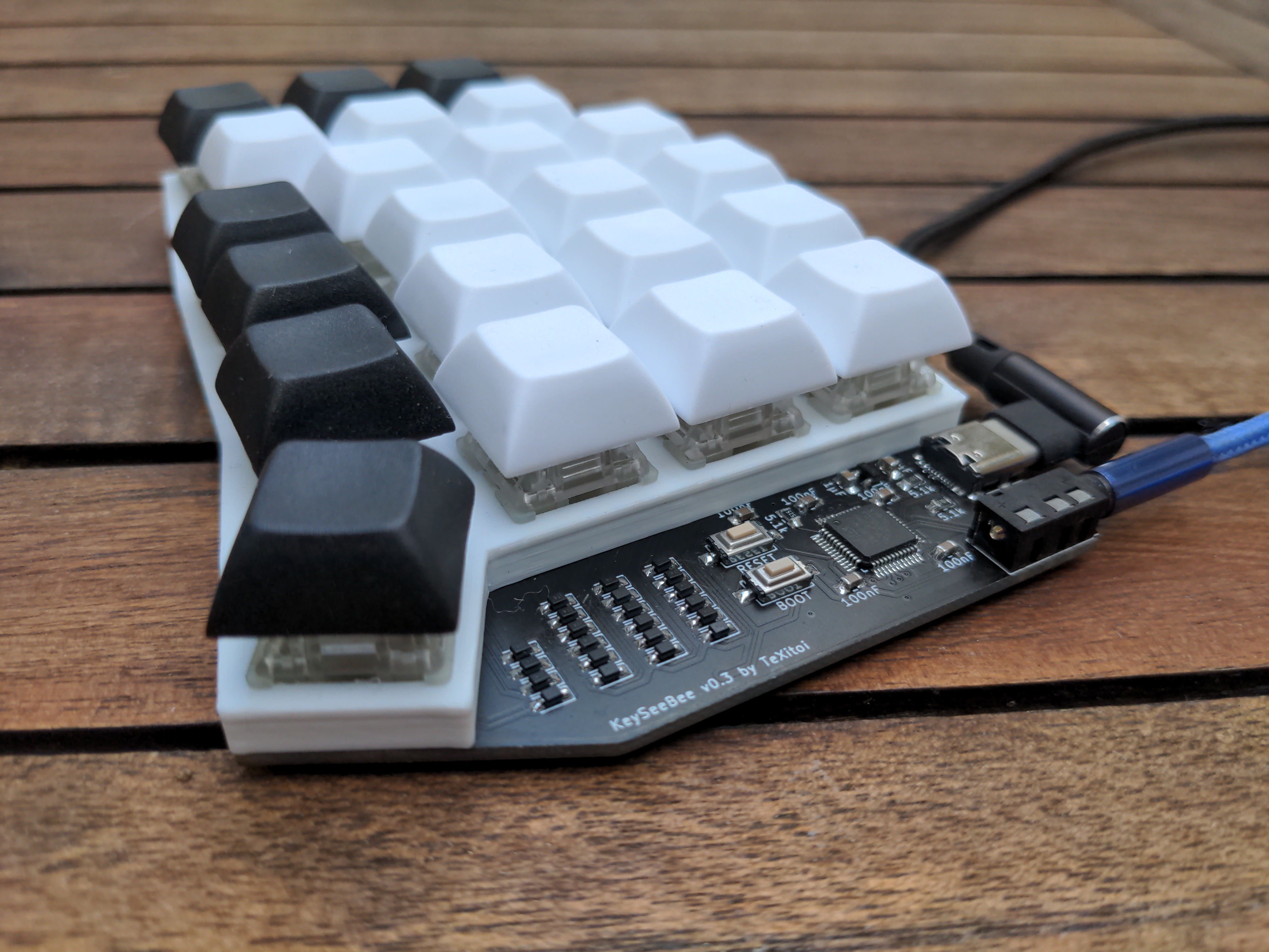
Price is for 5 keyboards including shipping.
| Item | Package | Qty | Remarks | Price |
|---|---|---|---|---|
| Left PCB | 1 | Ordered at JLCPCB | ||
| Right PCB | 1 | Ordered at JLCPCB | 33.14€ | |
| USB-C connector | 16 pins | 2 | 1.44€ | |
| 1N4148WS | SOD-323 | 44 | Price is for 1000 | 2.82€ |
| PJ320A TRRS connector | 2 | 1.01€ | ||
| STM32F072CBT6 MCU | LQFP-48 | 2 | STM32F072C8T6 would also work | 9.65€ |
| XC6206P332MR regulator | SOT-23 | 2 | Price is for 50 | 1.93€ |
| SMD switch | 3×6mm | 4 | Price is for 100 | 1.35€ |
| 5.1kΩ resistor | 0805 | 6 | Price is for 100 | |
| 1µF capacitor | 0805 | 4 | Price is for 100 | |
| 100nF capacitor | 0805 | 10 | Price is for 100 | 3.46€ |
| Bumpers | 5×2mm | 10 | Price is for 100 | 1.75€ |
| Cherry MX compatible or Kailh Choc switch | 5 pins (PCB mount) | 44 | ||
| 1U keycap compatible with the chosen switches | 44 | |||
| TRRS cable | Jack 3.5mm | 1 | 4 contacts needed | |
| USB-C cable | 1 | USB-2 is enough |
About 60€ without switches, keycaps and cables for 5 keyboards (12€/keyboard).
Install the complete toolchain and utils:
curl https://sh.rustup.rs -sSf | sh
rustup target add thumbv6m-none-eabi
rustup component add llvm-tools-preview
cargo install cargo-binutils
sudo apt-get install dfu-util
Compile:
cd firmware
cargo objcopy --bin keyseebee --release -- -O binary keyseebee.bin
To flash using dfu-util, launch it with:
dfu-util -w -d 0483:df11 -a 0 -s 0x08000000:leave -D keyseebee.binThen, put the board in dfu mode by pressing BOOT, pressing and releasing RESET and releasing BOOT. The upload should began as soon as the computer detect the board in dfu mode.
The first time, if the write fail, your flash might be protected. To unprotect:
dfu-util -d 0483:df11 -a 0 -s 0x08000000:force:unprotect -D keyseebee.binIdeally both sides needs to be flashed, but for changes that only affect the layout it's strictly not needed as the side connected with the USB cable will determine the layout. In fact, you can have different layouts stored on each half, meaning you can switch back and forth between two layouts by moving the USB cable between the two halves.
Here is the empty keyboard-layout-editor describing the layout.
I use the ergol layout, so this is the main layer when I type.
The layer 1 is activated by holding space.
The layer 2 is activated by holding Layer 2.
The layer 3
is activaded by holding space then Layer 2.
| Qty | Value | Footprint | References |
|---|---|---|---|
| 22 | 1N4148WS | Diode_SMD:D_SOD-323_HandSoldering | D10, D11, D12, D14, D15, D16, D17, D19, D20, D21, D23, D24, D25, D26, D33, D34 +6 |
| 22 | SW_Push | custom:CherryMX_Choc_1u | SW3, SW10, SW12, SW13, SW14, SW15, SW17, SW18, SW19, SW21, SW22, SW23, SW24, SW31, SW32, SW33 +6 |
| 5 | 100nF | Capacitor_SMD:C_0805_2012Metric_Pad1.15x1.40mm_HandSolder | C1, C2, C3, C4, C5 |
| 3 | 5.1k | Resistor_SMD:R_0805_2012Metric_Pad1.15x1.40mm_HandSolder | R1, R6, R7 |
| 2 | 1µF | Capacitor_SMD:C_0805_2012Metric_Pad1.15x1.40mm_HandSolder | C6, C7 |
| 1 | AudioJack4 | keebio:TRRS-PJ-320A-no-Fmask | J2 |
| 1 | BOOT | Button_Switch_SMD:SW_SPST_CK_RS282G05A3 | SW1 |
| 1 | Conn_01x12_Male | kicad-harwin:Harwin_M20-89012xx_1x12_P2.54mm_Horizontal | J3 |
| 1 | LDO | Package_TO_SOT_SMD:SOT-23 | U2 |
| 1 | RESET | Button_Switch_SMD:SW_SPST_CK_RS282G05A3 | SW2 |
| 1 | STM32 | Package_QFP:LQFP-48_7x7mm_P0.5mm | U1 |
| 1 | USB_C_Receptacle_USB2.0 | kicad-usb:USB_C_Receptacle_HRO_TYPE-C-31-M-12 | J1 |
It measures 135.9 × 89.5 mm and has 2 copper layers, 1.6 mm thick.
61 parts, built around the 1N4148WS. The full list of its parts is on this page, with links to each part's symbol and footprint where PCBKit's library has them.
From the TeXitoi/keyseebee repository on GitHub, at the commit this page was made from: the board is pcb/kicad/left/left.kicad_pcb. PCBKit opens the board in the browser, with nothing to install.
Its repository publishes it under the MIT licence: you may reuse it on that licence's terms (keep the author's notice, and for a copyleft licence share your changes alike).
TeXitoi/keyseebee
KeySeeBee is a split ergo keyboard. It is only 2 PCB (so the name) with (almost) only SMD components on it. It's only a keyboard, no LED, no display, nothing more than keys and USB.

shorepine/tulipcc
The Tulip Creative Computer and AMYboard - portable Python synthesizers

antmicro/jetson-nano-baseboard
Antmicro's open hardware baseboard for the NVIDIA Jetson Nano, TX2 NX and Xavier NX

Twisted-Fields/rp2040-motor-controller
A dual channel brushless motor controller based on the RP2040 microcontroller, designed in Kicad.


JanM321/esphome-lg-controller
Wired controller for LG HVAC units using ESPHome and ESP32

plinkysynth/plinky_public
a public release of the plinky sw and hw

TobleMiner/DC-UPS
A small DC UPS, designed to keep small appliances like consumer network equipment running during power outages
