Convertible keyboard PCB: full-size ISO-DE & ANSI with a snap-off numpad that turns it into a TKL (RP2040, USB-C, KiCad). Cheap, clean, modern core to build on — looking for a case designer.
Convertible keyboard pcb is an open-source printed circuit board by TechnikWeber, from the TechnikWeber/convertible-keyboard-pcb repository on GitHub. It is a 2-layer board of 431.2 × 126.4 mm with 504 parts on 282 nets, routed with 5,372 tracks and 906 vias.
It is built around the RP2040, W25Q16JVSSIQ and AP2112K-3.3TRG1, with the USBLC6-2SC6, 1N4148W and XL-3216UWC-FB among its other parts. Its parts include 218 diodes, 124 resistors, 110 switches, 18 capacitors and 4 ICs. It belongs with the keyboards and input boards and the RP2040 boards of this library.
This keyboard has a PCB in progress but no case yet. If you design keyboard
cases — 3D-printed, CNC-milled or laser-cut — and would like to take this on,
please open an issue.
A first board outline exists (key field + 1.3 mm), but outline, mounting holes
and the USB-C position can still be shaped around your case design — for the full-size board, the TKL, or
both. The same goes for where exactly the lock indicators sit. The USB port
can sit on the PCB or on a Unified Daughterboard (Pico-EZmate or JST-SH).
One keyboard PCB, two sizes. A full-size ISO-DE / ANSI board whose numpad
snaps off along a breakaway line. What remains is a complete tenkeyless (TKL)
keyboard — same PCB, same controller, same firmware.
This is not meant to be yet another one-off DIY keyboard. The goal is a
standardised core design that others can build on: cheap and simple to make, but
clean and modern — current KiCad, QMK, USB-C and parts that can actually be
bought. A case, lighting or layout variants build on this core instead of
bending it into something else.
Status: early. The schematic is complete — key matrix, ANSI alternatives,
backlight and controller — and every part has its footprint on the PCB.
Controller, USB and drivers are placed on the back, board outline and breakaway
line are drawn; mounting holes and routing are still to do.
Nothing has been manufactured yet.
Full-size or TKL
The numpad sits on the right-hand side behind a 2 mm slot, held by four
mouse-bite tabs (perforated breakaway bridges). Each tab keeps a hole-free
channel in the middle for the traces that cross over.
Controller, USB-C and the drivers for backlight and lock indicators all sit
on the TKL part. Only the numpad's matrix, backlight and indicator lines cross the breakaway
line.
Snap the numpad off and the TKL keeps working unchanged — the numpad keys are
simply gone. The firmware describes both layouts.
The lock indicators above the numpad go with it – without a numpad Num Lock is
pointless anyway; for the TKL populate the Caps Lock indicator above Page Up.
The snapped-off numpad has no controller of its own and does not work on its
own.
Specs
Full-size: 105 keys ISO-DE, key field 428.6 × 123.8 mm (22.5 × 6.5 u)
TKL: 88 keys ISO-DE, key field 347.7 × 123.8 mm (18.25 × 6.5 u)
ISO-DE and ANSI on one PCB: alternative positions for Enter, left Shift and
backslash (the ANSI backslash is the only key without an LED)
Cherry MX-compatible switches, soldered, with stabilizer holes on all keys of
2u and wider
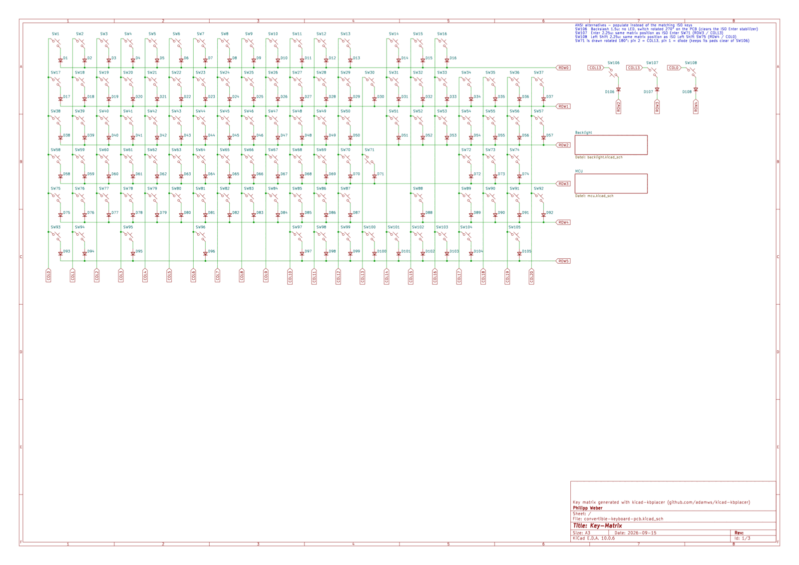
6 × 21 diode matrix (SOD-123)
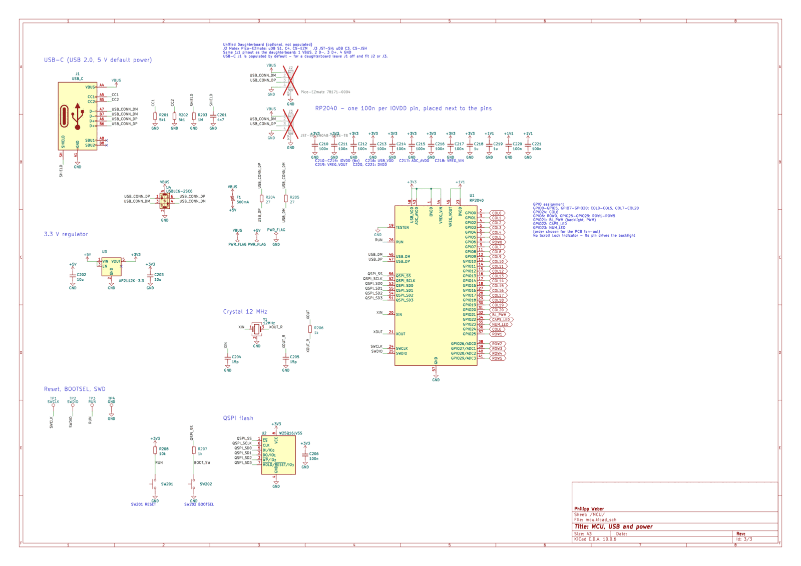
RP2040 controller with 16 Mbit QSPI flash, RESET and BOOTSEL buttons and SWD
test pads
USB-C (USB 2.0) on the board with ESD protection, 500 mA polyfuse and a 3.3 V
LDO – or a Unified Daughterboard instead: connectors for Molex Pico-EZmate
(uDB S1, C4, C5-EZM) and JST-SH (uDB C3, C5-JSH) are provided, not populated
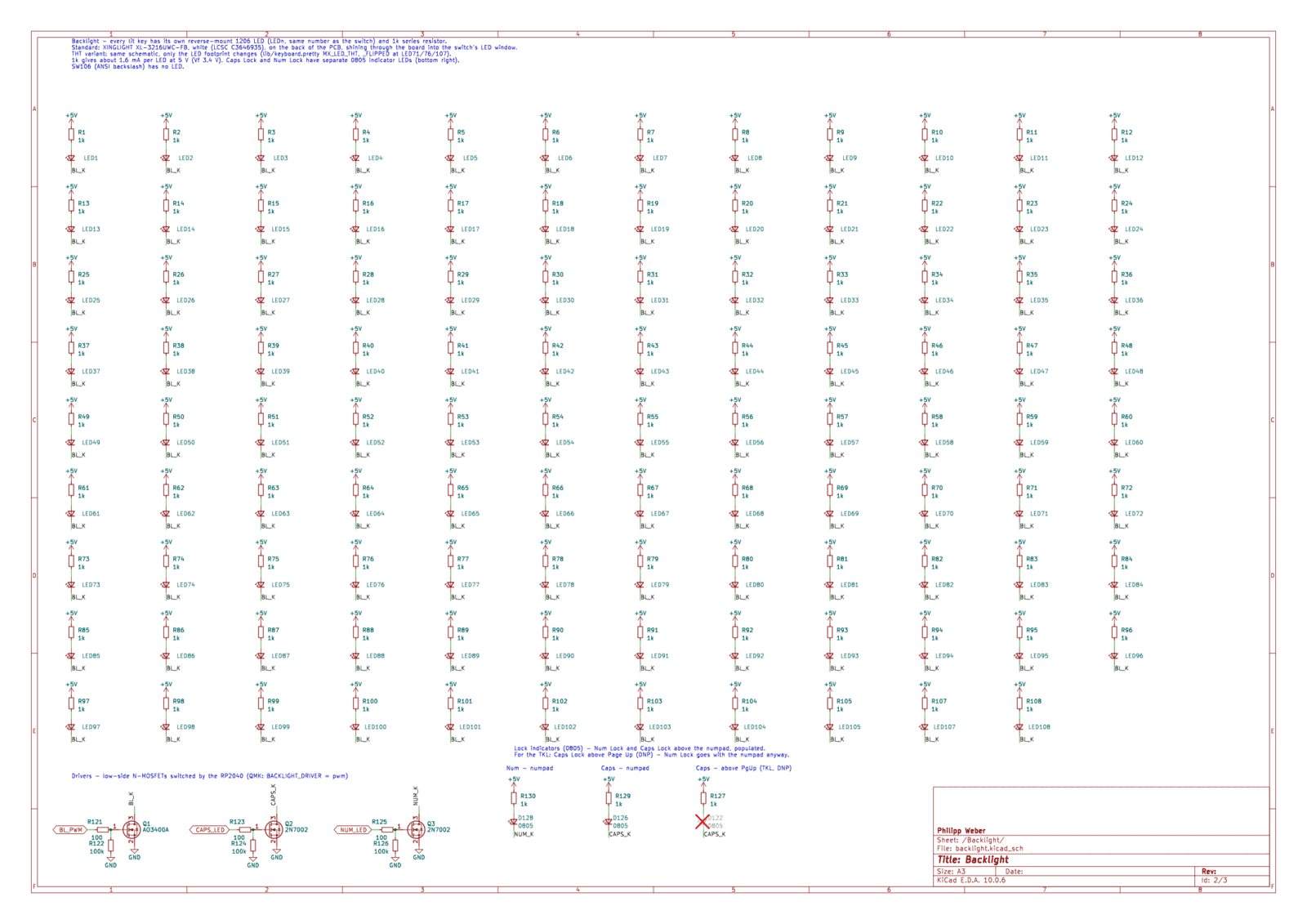
Single-colour backlight with reverse-mount 1206 LEDs on the back of the PCB
(white, XINGLIGHT XL-3216UWC-FB), machine-assembled; switched, dimmed and
"breathing" via QMK. A THT-LED variant uses the same design with different LED
footprints
Checked alternative backlight LEDs for the same footprint: MEIHUA MHT151WDT
(LCSC C401114) and TUOZHAN P2-1206WYCS2-0.9T-F (LCSC C2827252)
Caps Lock and Num Lock indicators (0805) above the numpad; for the TKL a Caps
Lock indicator above Page Up is prepared but not populated
All 30 RP2040 GPIOs in use: 27 matrix lines, backlight PWM, Caps Lock and
Num Lock
Repository
Path
Contents
convertible-keyboard-pcb.kicad_pro / .kicad_pcb
KiCad 10 project and PCB
convertible-keyboard-pcb.kicad_sch
Root sheet: key matrix and ANSI alternatives
backlight.kicad_sch
Key LEDs, series resistors and MOSFET drivers
mcu.kicad_sch
RP2040, flash, crystal, USB-C and power
lib/keyboard.pretty
Project footprints: reverse-mount LED, THT LED for the variant
fp-lib-table, convertible-keyboard-pcb.kicad_dru
Footprint library table, design rule for the LED cutouts
lib/MX_Alps_Hybrid
Switch footprints by ai03 (git submodule)
tools/
Scripts that generated the sheets and updated the PCB – see tools/README.md
docs/production/
Gerbers, drill file, BOM and placement file for JLCPCB
These renders let you review the design without installing KiCad.
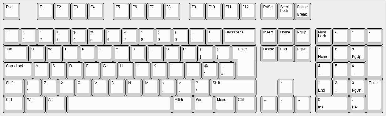
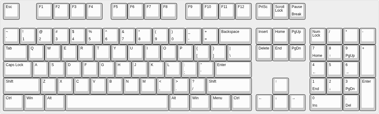
Key layouts
Everything is built around these two: ISO-DE with 105 keys and ANSI with 104. The board carries both. The ANSI
positions are alternative footprints that stay unpopulated on an ISO build, and the other way round.
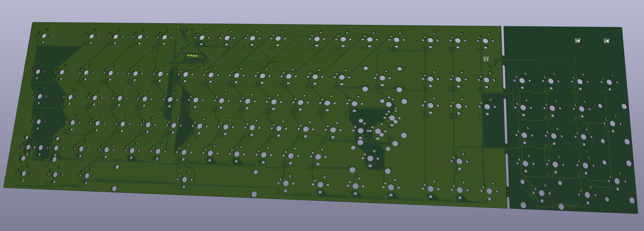
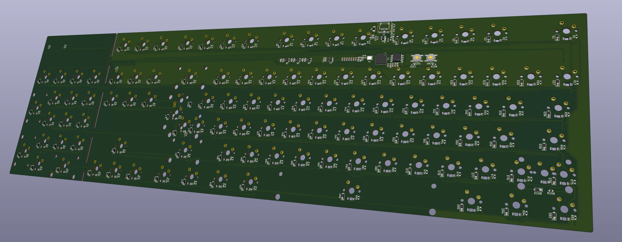
Board in 3D
Switch side: through holes for the switches and their stabilisers, no components. Note the breakaway line in
front of the numpad.
Component side: nearly everything sits here. Diodes and resistors per key, the reverse-mount LEDs shining
through their cutouts, and the controller in the gap between F4 and F5. The only parts on the other side are
the two lock indicators above the numpad.
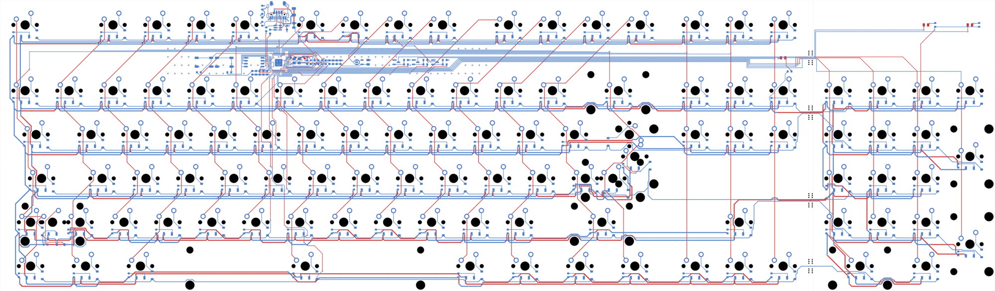
Board
Both copper layers, zone fills hidden so the traces stay readable. The numpad on the right snaps off along the
breakaway line; only matrix lines, +5V, BL_K and the two lock-LED lines cross it, through the four tabs.
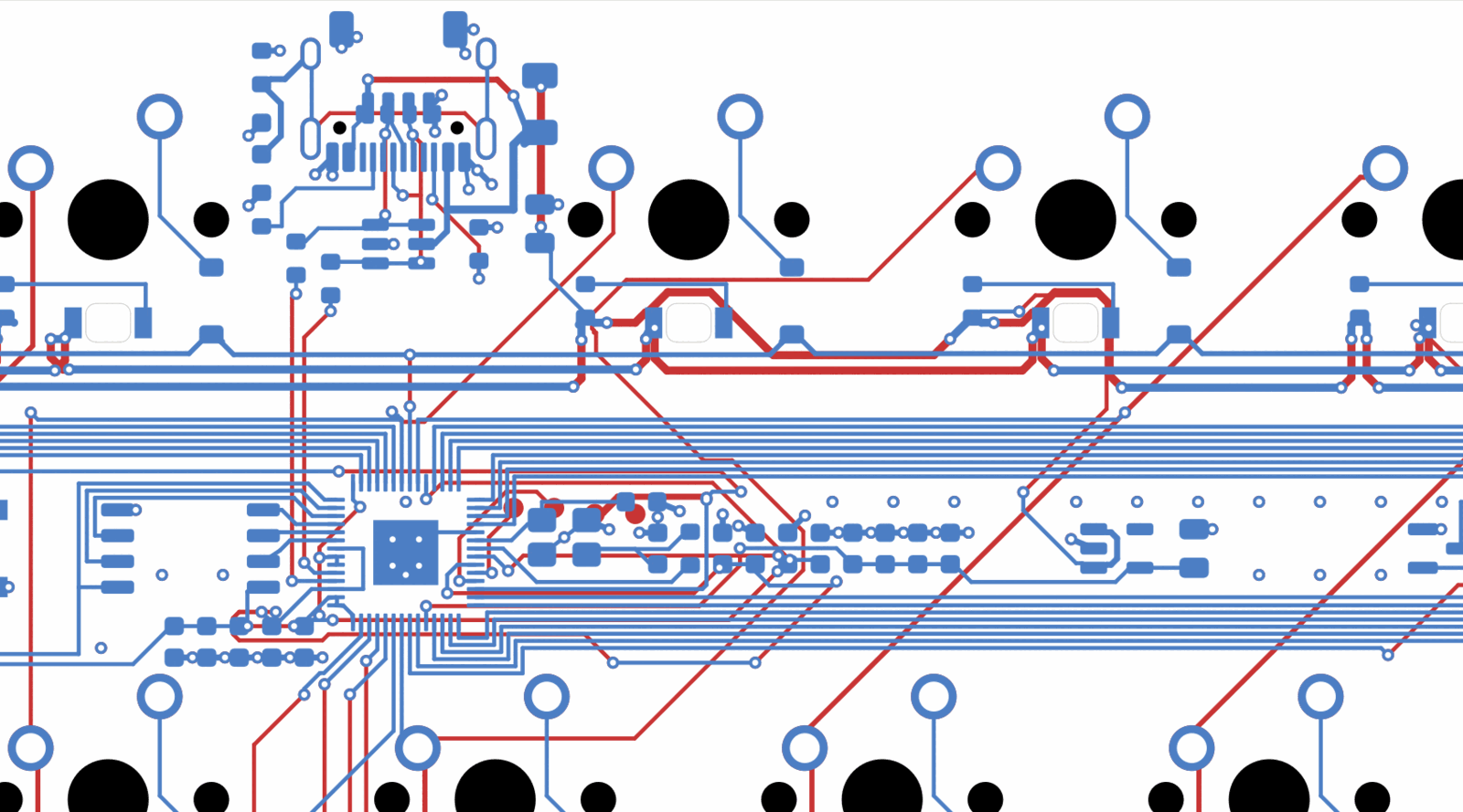
The controller sits in the gap between F4 and F5. Column and row buses run in fixed lanes and each one ends on a
via that drops onto the column trace of its key. Every SMD part in this area is on the back.
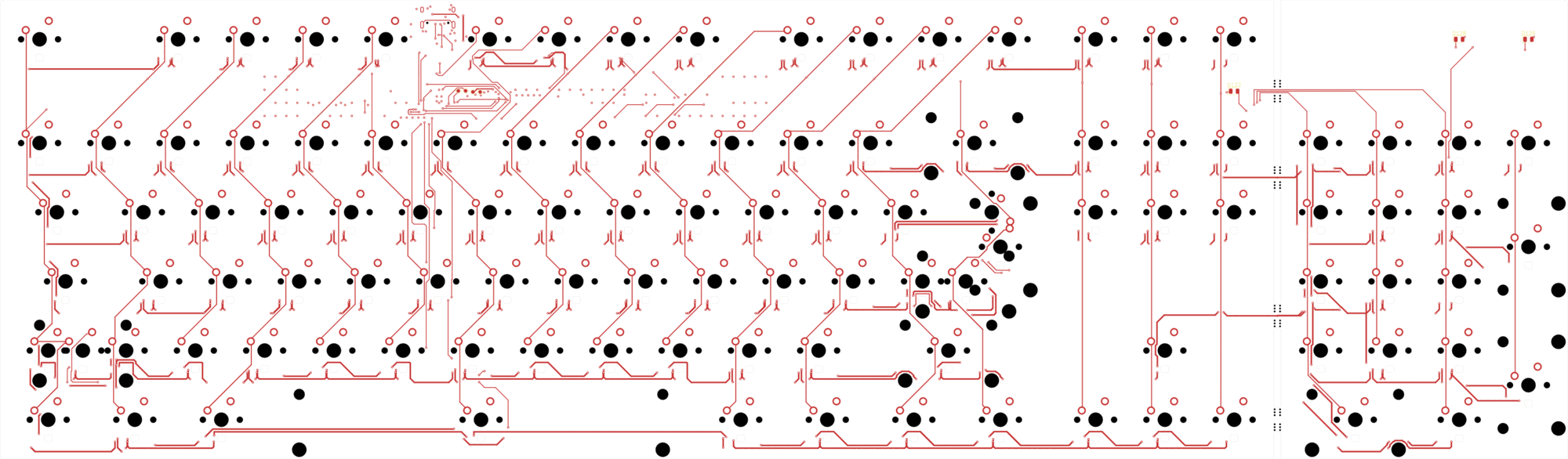
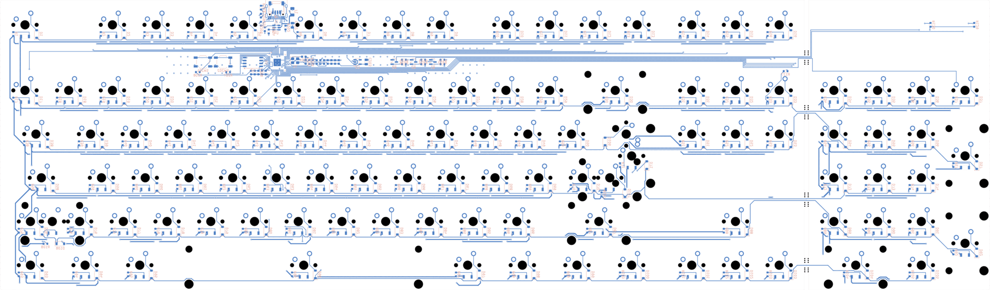
Front (switch side, mostly through holes and the key matrix) and back (all components, reverse-mount LEDs):
Schematic
Key matrix with the ANSI alternatives:
Backlight, lock indicators and their drivers:
Controller: RP2040, flash, crystal, LDO, USB-C with ESD protection, daughterboard connectors, buttons, test pads:
Having it made
Gerbers, drill file, BOM and placement file for JLCPCB are in
docs/production/, all generated from the KiCad project. The board is
431.225 × 126.425 mm on two layers. 371 parts are machine-assembled; the 108 MX switches are soldered by
hand, and three parts are deliberately left unpopulated.
JLCPCB's minimum order is 5 boards: $45 for five bare PCBs, or $112 for five with two of them
assembled (checked 2026-09-16, shipping in, customs out). Switches, keycaps and a case come on top.
Nothing here has been built in hardware yet. The files pass DRC and schematic parity, nothing more —
review them before you spend money.
Mounting holes: 14 × M2, placed in the free areas; final positions together with the case designer
Placement of controller, USB and drivers (preliminary)
Routing complete: key matrix and controller area (DRC clean, schematic parity clean, no open nets)
Manufacturing files for JLCPCB: gerbers, drill, BOM and placement file, an LCSC number on every part
Firmware (QMK): four layouts (full-size and TKL, each ISO and ANSI), matrix generated from the
board file, backlight and lock indicators; compiles, not yet run on hardware
License
CC-BY-NC-SA-4.0, notes in NOTICE.md. The switch footprints in
lib/MX_Alps_Hybrid are by ai03 under the MIT License;
the THT LED footprints in lib/keyboard.pretty use their pad geometry.
A modern remake of the Bare Conductive Touch Board: 12 capacitive touch electrodes, MP3/WAV/MIDI audio, and now WiFi, Bluetooth LE, USB-C, a proper LiPo power path, a fuel gauge, line-in, MIDI out, Qwiic and an RGB LED.
A lightweight, rechargeable two-key fidget that counts clicks, resets with a second key, and remembers its count while asleep or unpowered. Designed for a home-printed enclosure and professionally assembled electronics.
96 parts
Questions
How big is the Convertible keyboard pcb PCB?
It measures 431.2 × 126.4 mm and has 2 copper layers, 1.6 mm thick.
What parts does the Convertible keyboard pcb use?
504 parts, built around the RP2040, W25Q16JVSSIQ, AP2112K-3.3TRG1 and USBLC6-2SC6. The full list of its parts is on this page, with links to each part's symbol and footprint where PCBKit's library has them.
Where can I download the Convertible keyboard pcb KiCad files?
From the TechnikWeber/convertible-keyboard-pcb repository on GitHub, at the commit this page was made from: the board is convertible-keyboard-pcb.kicad_pcb and its schematic backlight.kicad_sch. PCBKit opens the board in the browser, with nothing to install.
Can I use the Convertible keyboard pcb design in my own project?
Its repository states no licence, so its author keeps all rights: ask TechnikWeber before reusing the design.