
2 layers78.7 × 58.4 mm

 techmiguel/smartRele
Single-channel Wi-Fi relay module based on the ESP-12F (ESP8266) for 110–120 VAC and loads up to 10 A. Open hardware in KiCad 10, ready for full assembly at JLCPCB.
Rele esp12f is an open-source printed circuit board by techmiguel, from the techmiguel/smartRele repository on GitHub, published under the CERN-OHL-W-2.0 licence. It is a 2-layer board of 66.5 × 49 mm with 34 parts on 31 nets, routed with 123 tracks and 36 vias.
It is built around the ESP-12F, HLK-PM01 and AMS1117-3.3, with the TS-1187A-B-A-B, 07D221K and 1N4148W among its other parts. Its parts include 9 capacitors, 9 resistors, 3 diodes, 3 switches and 2 ICs. It belongs with the home automation and IoT boards and the ESP8266 boards of this library.


Single-channel Wi-Fi relay module based on the ESP-12F (ESP8266) for 110–120 VAC mains.






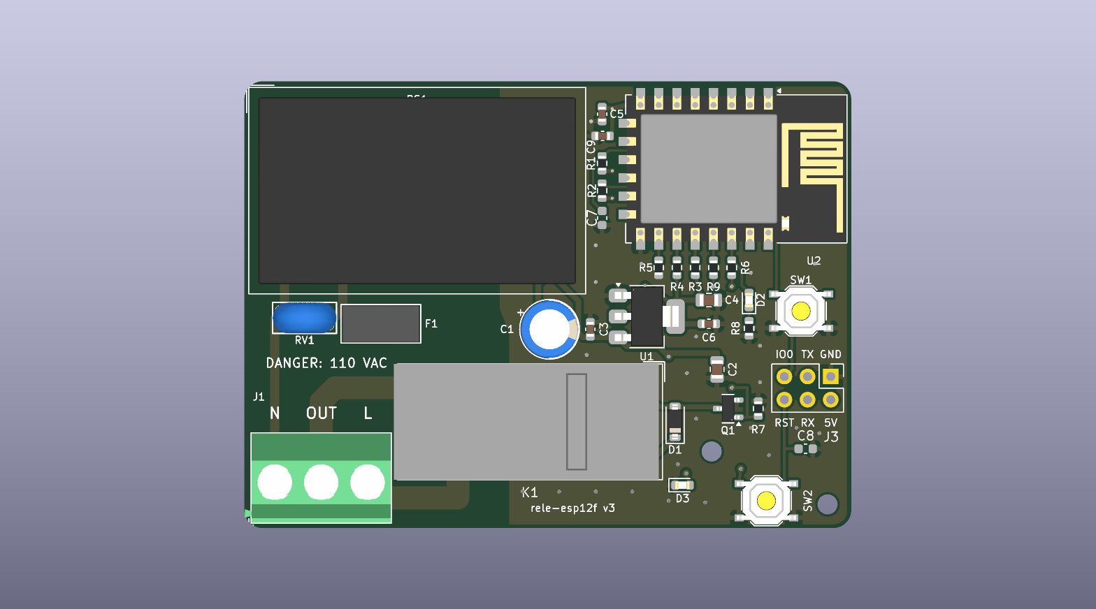
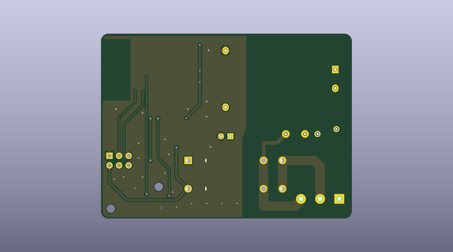
A 2-layer, 66.5 × 49 mm board that switches a mains load of up to 10 A from an ESP-12F. It is powered directly from the mains through an isolated HLK-PM01 supply and integrates input protection (time-lag fuse and varistor), a 16 A Omron G5RL power relay, status indicators and a programming header. All components sit on the top side, and the board is ready to be ordered fully assembled from JLCPCB (SMD and THT), with no hand soldering.
[!WARNING] This design operates at mains voltage. Assembly, testing and installation must be carried out by qualified people. Read the Safety section before connecting the board.
| Parameter | Value |
|---|---|
| Input voltage | 110–120 VAC, 50/60 Hz |
| Maximum load | 10 A resistive (trace limit; relay 16 A, terminal block 18 A) |
| Contact | SPST-NO, switches the line (L) |
| On-board supply | HLK-PM01, 5 V / 600 mA, isolated |
| Regulator | AMS1117-3.3 |
| Microcontroller | ESP8266 (ESP-12F module), Wi-Fi 802.11 b/g/n |
| Protection | F1 T500mA 250 V (supply branch) · RV1 07D221K |
| PCB | 66.5 × 49 × 1.6 mm, 2 layers, 35 µm copper |
| Assembly | Single-sided; 32 components, all factory-assembled |
| Mounting holes | 2 × M2 (MH1, MH2), in the low-voltage zone |
The full datasheet, with test conditions and the source of each value, is in docs/rele-esp12f_datasheet_user_guide.pdf.
 Power      J1:L ──────────► K1 contact (COM → NO) ──────────► J1:OUT ──► load

 Supply     J1:L ── F1 ── L_F ──► PS1 HLK-PM01 ──► +5 V ── U1 AMS1117 ──► +3.3 V ──► U2 ESP-12F
                          RV1 between L_F and N

 Control    +5 V ── K1 coil (D1 flyback diode) ── Q1 SS8050 ── GND
                                                   ▲
GPIO5 (U2) ── R6 1 kΩThe full schematic is in docs/schematic.pdf.
| Pin | Signal | Function |
|---|---|---|
| 1 | N | Neutral |
| 2 | OUT | Switched output to the load |
| 3 | L | Line input |
 IO0   TX   GND(1)
 RST   RX   5V
Pin 1 (square pad) = GND; pin 2 = 5 V. Labeled on the silkscreen.
| GPIO | Function |
|---|---|
| GPIO5 | Relay (SS8050, R6 1 kΩ, R7 10 kΩ to GND) and relay LED (D2) |
| GPIO4 | Wi-Fi LED (D3) |
| GPIO0 | Push button SW1 (flashing mode / application use), 10 kΩ to 3.3 V |
| GPIO2 | 10 kΩ to 3.3 V (boot strap) |
| GPIO15 | 10 kΩ to GND (boot strap) |
| EN, RST | 10 kΩ to 3.3 V + 100 nF to GND; RST also to SW2 |
.
├── rele-esp12f.kicad_pro      KiCad 10 project
├── rele-esp12f.kicad_sch      Schematic
├── rele-esp12f.kicad_pcb      PCB layout
├── rele-esp12f.kicad_dru      Custom design rules (mains isolation)
├── 3dmodels/                  STEP models missing from the KiCad library (K1, F1, SW1/SW2)
├── fabrication/               Production package for JLCPCB
│   ├── gerbers/               Gerbers and drill files (Excellon)
│   ├── gerbers_JLCPCB.zip     Gerbers + drill files + CPL, ready to upload
│   ├── BOM_JLCPCB.csv         Bill of materials with LCSC part numbers
│   └── CPL_JLCPCB.csv         Component placement list
├── docs/
│   ├── schematic.pdf
│   ├── rele-esp12f_datasheet_user_guide.pdf
│   ├── pcb_top.png · pcb_bottom.png
│   └── datasheets/            Datasheets of the key components
├── firmware/                  ESP8266 firmware (PlatformIO, Arduino core)
├── enclosure/                 3D-printable enclosure (FreeCAD, STEP, STL)
├── scripts/                   PDF datasheet generator
├── CHANGELOG.md
└── LICENSE
The custom 3D models are referenced through ${KIPRJMOD}/3dmodels/, so the project opens without any extra path configuration.
fabrication/gerbers_JLCPCB.zip to JLCPCB (2 layers, 1.6 mm).BOM_JLCPCB.csv and CPL_JLCPCB.csv.THT parts are wave-soldered. The CPL uses the pad center (JLCPCB convention), not the body center; for U2 and K1 they differ. The drill holes of J1 (Ø1.5 mm) and RV1 (Ø1.0 mm) are matched to the actual parts.
| Ref. | Part | LCSC | Notes |
|---|---|---|---|
| PS1 | Hi-Link HLK-PM01 | C209903 | Isolated 5 V supply |
| K1 | Omron G5RL-1A-E-HR DC5 | C113250 | SPST-NO 16 A; 5 V coil, 80 mA |
| F1 | Reomax MTS0500A, T500mA 250 V | C2762401 | Time-lag, due to the PS1 inrush current |
| RV1 | Varistor 07D221K | C49072913 | For 110–120 VAC |
| C1 | 470 µF 10 V | C112505 | |
| J1 | KANGNEX WJ500V-5.08-3P | C72334 | 250 V / 18 A |
| J3 | 2×3 header, 2.54 mm | C65114 | Only used for the first flashing |
The full list is in the BOM.
With kicad-cli (KiCad 10), from the repository root:
kicad-cli pcb export gerbers --layers F.Cu,B.Cu,F.SilkS,B.SilkS,F.Mask,B.Mask,F.Paste,Edge.Cuts -o fabrication/gerbers/ rele-esp12f.kicad_pcbkicad-cli pcb export drill --format excellon --excellon-units mm --excellon-separate-th --excellon-zeros-format decimal -o fabrication/gerbers/ rele-esp12f.kicad_pcbkicad-cli pcb render --side top -w 1592 -h 904 --background opaque --quality basic --zoom 0.9954 -o docs/pcb_top.png rele-esp12f.kicad_pcbkicad-cli pcb render --side bottom -w 1592 -h 904 --background opaque --quality basic --zoom 0.9954 -o docs/pcb_bottom.png rele-esp12f.kicad_pcbThese explicit options are needed because the plot settings stored in the board produce .gbr extensions and an unnecessary B.Paste layer. The ZIP contains the 11 files in fabrication/gerbers/ plus CPL_JLCPCB.csv.
The firmware/ folder holds the board's own firmware (PlatformIO, Arduino core for ESP8266). In this version the relay is controlled over Wi-Fi only, from a built-in web page or a JSON REST API:
On first boot it opens the SmartRele-XXXXXX setup access point; holding SW1 for 8 s erases the Wi-Fi settings. Setup, behaviour, API and security notes are in firmware/README.md.
pio run -e esp12f -t upload from firmware/). Later updates are done over the air (OTA).J3 is powered at 5 V rather than 3.3 V for two reasons. The internal output-to-input diode of the AMS1117 would make the adapter also feed the 5 V rail. In addition, the 3.3 V pin of a typical adapter cannot supply the current peaks the ESP8266 draws while calibrating its radio.
Third-party firmware also works: the datasheet includes example configurations for Tasmota and ESPHome.
The enclosure/ folder contains a two-part enclosure (base and screwed lid) for 3D printing in PETG or ASA/ABS. It is generated by a parametric FreeCAD script, and its interference with the 3D model of the assembled board is zero. Design, printing and assembly details are in enclosure/README.md.
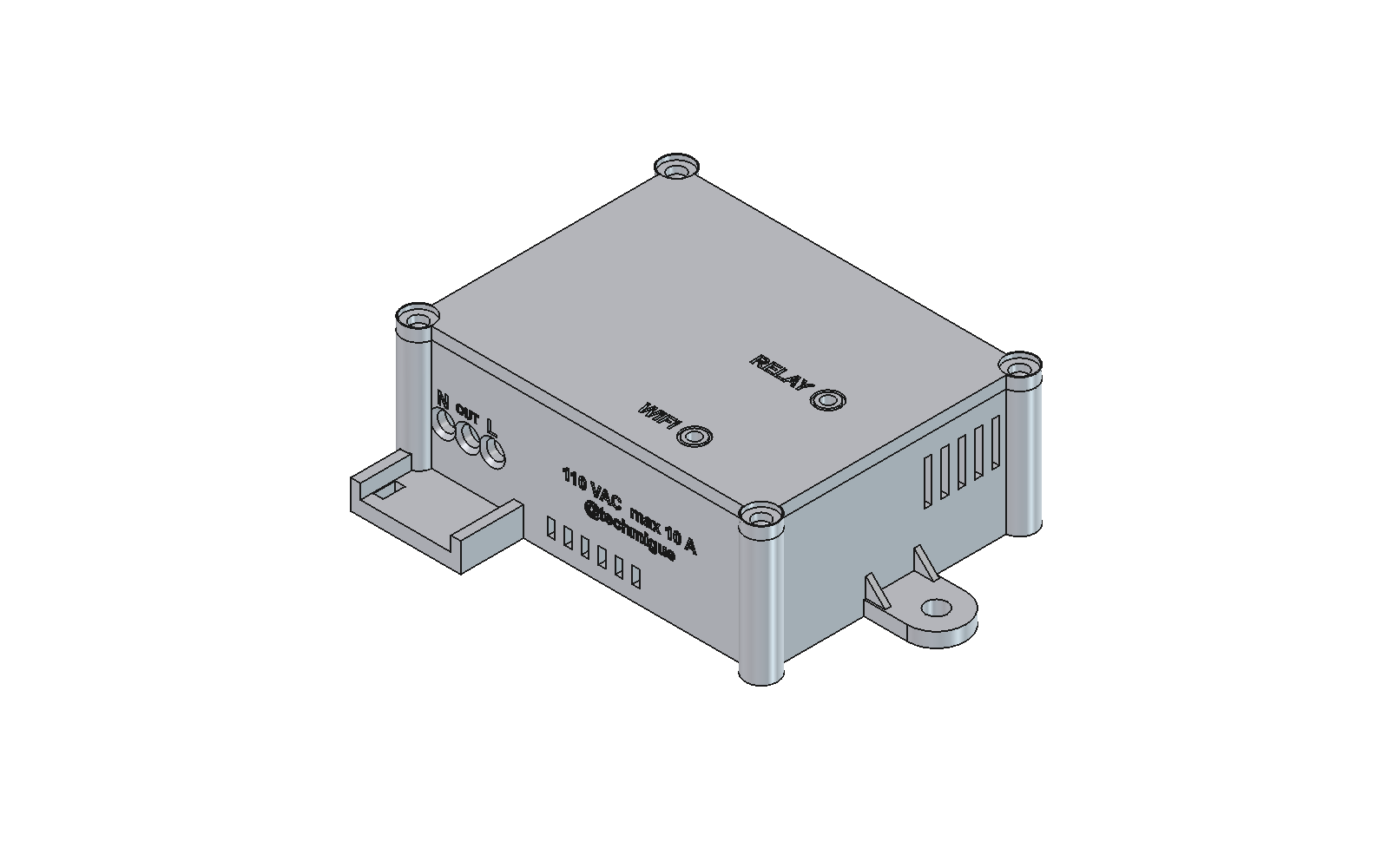
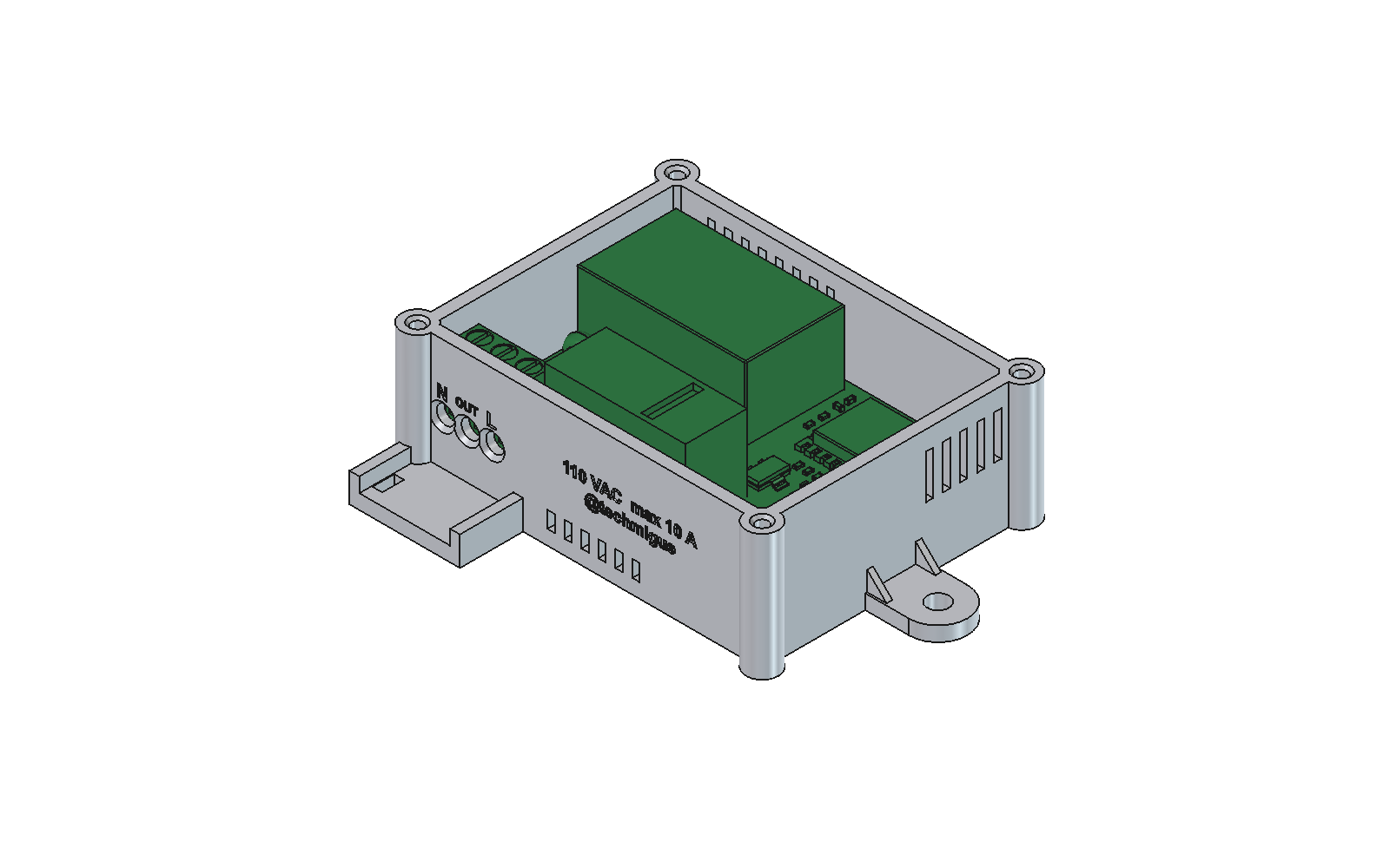
Results with kicad-cli 10.0.5, with all zones refilled:
| Check | Errors | Warnings | Warning details |
|---|---|---|---|
| DRC | 0 | 29 | 23 footprints modified from the library (J1/RV1 drills and custom 3D models); 6 PS1/J1 silkscreen items next to the rounded corners |
| Schematic ↔ PCB parity | 0 | 34 | 32 LCSC/assembly fields not copied to footprints; 2 mounting holes without a symbol |
| ERC | 0 | 9 | Off-grid endpoints and symbols that differ from the library |
| Unconnected pads | 0 | — |
None of the warnings affects manufacturing. Measured clearances: mains copper ↔ low voltage ≥ 4.35 mm on both sides; mains copper ↔ board edge ≥ 2.0 mm.
| Document | Contents |
|---|---|
| Datasheet and user guide | Specifications, operation, installation and design rationale |
| Schematic | Full schematic in PDF |
| Datasheets | Omron G5RL, AMS1117, ESP8266EX, ESP-WROOM-02 and the Espressif hardware design guidelines |
| Changelog | Hardware revisions and the rationale behind each change |
| Enclosure | Enclosure design, printing and assembly |
The datasheet is regenerated with python scripts/generate_datasheet.py (requires ReportLab, PyMuPDF, Pillow and kicad-cli).
Hardware released under the CERN Open Hardware Licence v2 – Weakly Reciprocal (CERN-OHL-W-2.0).
Inspired by aman983/ESP-01S_Relay_Module. This is a new design and contains no files from the original.
© 2026 @techmigue
| Qty | Value | Footprint | References |
|---|---|---|---|
| 6 | 10k | Resistor_SMD:R_0603_1608Metric | R1, R2, R3, R4, R5, R7 |
| 5 | 100nF | Capacitor_SMD:C_0603_1608Metric | C3, C5, C6, C7, C8 |
| 2 | 1k | Resistor_SMD:R_0603_1608Metric | R6, R8 |
| 2 | 22uF 10V | Capacitor_SMD:C_0805_2012Metric | C2, C4 |
| 2 | M2 | MountingHole:MountingHole_2.2mm_M2 | MH1, MH2 |
| 2 | TS-1187A | Button_Switch_SMD:SW_Push_1P1T_XKB_TS-1187A | SW1, SW2 |
| 1 | 07D221K | Varistor:RV_Disc_D7mm_W3.4mm_P5mm | RV1 |
| 1 | 10uF | Capacitor_SMD:C_0603_1608Metric | C9 |
| 1 | 1N4148W | Diode_SMD:D_SOD-123 | D1 |
| 1 | 220 | Resistor_SMD:R_0603_1608Metric | R9 |
| 1 | 470uF 10V | Capacitor_THT:CP_Radial_D6.3mm_P2.50mm | C1 |
| 1 | AMS1117-3.3 | Package_TO_SOT_SMD:SOT-223-3_TabPin2 | U1 |
| 1 | ESP-12F | RF_Module:ESP-12E | U2 |
| 1 | G5RL-1A-E-HR DC5 | Relay_THT:Relay_SPST_Omron_G2RL-1A-E | K1 |
| 1 | HLK-PM01 | Converter_ACDC:Converter_ACDC_Hi-Link_HLK-PMxx | PS1 |
| 1 | LED WiFi (blue) | LED_SMD:LED_0603_1608Metric | D3 |
| 1 | LED relay (red) | LED_SMD:LED_0603_1608Metric | D2 |
| 1 | N / L_OUT / L_IN | TerminalBlock_Phoenix:TerminalBlock_Phoenix_MKDS-1,5-3-5.08_1x03_P5.08mm_Horizontal | J1 |
| 1 | PROG | Connector_PinHeader_2.54mm:PinHeader_2x03_P2.54mm_Vertical | J3 |
| 1 | SS8050 | Package_TO_SOT_SMD:SOT-23 | Q1 |
| 1 | T500mA 250V | Fuse:Fuse_Littelfuse_395Series | F1 |
It measures 66.5 × 49 mm and has 2 copper layers, 1.6 mm thick.
34 parts, built around the ESP-12F, HLK-PM01, AMS1117-3.3 and TS-1187A-B-A-B. The full list of its parts is on this page, with links to each part's symbol and footprint where PCBKit's library has them.
From the techmiguel/smartRele repository on GitHub, at the commit this page was made from: the board is rele-esp12f.kicad_pcb and its schematic rele-esp12f.kicad_sch. PCBKit opens the board in the browser, with nothing to install.
Its repository publishes it under the CERN-OHL-W-2.0 licence: you may reuse it on that licence's terms (keep the author's notice, and for a copyleft licence share your changes alike).


venkatesh3549/STM32-Based-Smart-Energy-Meter-PCB-Design
ustom 2-layer PCB design for an STM32-based Smart Energy Meter with voltage/current monitoring and Wi-Fi communication, developed using KiCad."

VinayGopi-PK/ESP32-4-Channel-WiFi-Home-Automation
ESP32-based 4-channel Wi-Fi Home Automation Controller designed in KiCad. Includes schematic, PCB layout, Gerber files, BOM and 3D visualization.

whysixmift/smarthome_v0.1
I wanted to control lights and appliances in my room over Wi-Fi without having loose relay modules, breadboards, and 220V AC wires floating around my desk.


alextrical/ESP8266-Sentinel-Kinetic-Wired-Remote
ESP8266 based Re-implementation of the Vent-Axia Sentinel Kinetic Wired Remote Controller

Robast-GmbH/PCB_Designs
This repository contains all the necessary files and instructions for the PCBs that are designed using KiCad. Here is an overview of the main components: - .github: Contains Github-specific configurations, including…